LDP (HL),HL
LDP (IX),HL
LDP (IY),HL
|
|
|
| ED 64 |
LDP (HL),HL |
12 (2,2,2,3,3) |
(HL) = L; (HL + 1) = H. (Addr[19:16] = A[3:0]) |
| DD 64 |
LDP (IX),HL |
12 (2,2,2,3,3) |
(IX) = L; (IX + 1) = H. (Addr[19:16] = A[3:0]) |
| FD 64 |
LDP (IY),HL |
12 (2,2,2,3,3) |
(IY) = L; (IY + 1) = H. (Addr[19:16] = A[3:0]) |
Description
These instructions are used to access 20-bit addresses. In all cases, the four most significant bits of the 20-bit
address (bits 19 through 16) are defined as the four least significant bits of A (bits 3 though 0). The LDP
instructions bypass the MMU's address translation unit for direct access to the 20-bit memory address space.
-
LDP (HL),HL: Loads the memory location whose 16 least significant bits of its 20-bit address are the data in HL with the data in L, and then loads the following 20-bit address with the data in H.
-
LDP (IX),HL: Loads the memory location whose 16 least significant bits of its 20-bit address are the data in IX with the data in L, and then loads the following 20-bit address with the data in H.
-
LDP (IY),HL: Loads the memory location whose 16 least significant bits of its 20-bit address are the data in IY with the data in L, and then loads the following 20-bit address with the data in H.
Note that the LDP instructions wrap around on a 64K page boundary. Since the LDP instruction operates on
two-byte values, the second byte will wrap around and be written at the start of the page if you try to read or
write across a page boundary. Thus, if you fetch or store at address 0xn,0xFFFF, you will get the bytes
located at 0xn, 0xFFFF and 0xn,0x0000 instead of 0xn,0xFFFF and 0x(n+1),0x0000 as you might expect.
Therefore, do not use LDP at any physical address ending in 0xFFFF.
LDP (mn),HL
LDP (mn),IX
LDP (mn),IY
|
|
|
| ED 65 n m |
LDP (mn),HL |
|
(mn) = L; (mn + 1) = H.
(Addr[19:16] = A[3:0]) |
| DD 65 n m |
LDP (mn),IX |
|
(mn) = IX(low); (mn + 1) = IX(high). (Addr[19:16] = A[3:0]) |
| FD 65 n m |
LDP (mn),IY |
|
(mn) = IY(low); (mn + 1) = IY(high). (Addr[19:16] = A[3:0]) |
*Clocking: 15 (2,2,2,2,1,3,3) |
Description
These instructions are used to access 20-bit addresses. In all cases, the four most significant bits of the 20-bit
address (bits 19 through 16) are defined as the four least significant bits of A (bits 3 though 0). The LDP
instructions bypass the MMU's address translation unit for direct access to the 20-bit memory address space.
-
LDP (mn),HL: Loads the memory location whose 16 least significant bits of its 20-bit address are the 16-bit constant mn with the data in L, and then loads the following memory location with the data in H.
-
LDP (mn),IX: Loads the memory location whose 16 least significant bits of its 20-bit address are the 16-bit constant mn with the low order byte of IX, and then loads the following memory location with the high order byte of IX.
-
LDP (mn),IY: Loads the memory location whose 16 least significant bits of its 20-bit address are the 16-bit constant mn with the low order byte of IY, and then loads the following memory location with the high order byte of IY.
Note that the LDP instructions wrap around on a 64K page boundary. Since the LDP instruction operates on
two-byte values, the second byte will wrap around and be written at the start of the page if you try to read or
write across a page boundary. Thus, if you fetch or store at address 0xn,0xFFFF, you will get the bytes
located at 0xn, 0xFFFF and 0xn,0x0000 instead of 0xn,0xFFFF and 0x(n+1),0x0000 as you might expect.
Therefore, do not use LDP at any physical address ending in 0xFFFF.
LDP HL,(HL)
LDP HL,(IX)
LDP HL,(IY)
|
|
|
| ED 6C |
LDP HL,(HL) |
10 (2,2,2,2,2) |
L = (HL); H = (HL + 1). (Addr[19:16] = A[3:0]) |
| DD 6C |
LDP HL,(IX) |
10 (2,2,2,2,2) |
L = (IX); H = (IX + 1). (Addr[19:16] = A[3:0]) |
| FD 6C |
LDP HL,(IY) |
10 (2,2,2,2,2) |
L = (IY); H = (IY + 1). (Addr[19:16] = A[3:0]) |
Description
These instructions are used to access 20-bit addresses. In all cases, the four most significant bits of the 20-bit
address (bits 19 through 16) are defined as the four least significant bits of A (bits 3 though 0). The LDP
instructions bypass the MMU's address translation unit for direct access to the 20-bit memory address space.
-
LDP HL,(HL): Loads L with the data whose 16 least significant bits of its 20-bit address are the data in HL, and then loads H with the data in the following 20-bit address.
-
LDP HL,(IX): Loads L with the data whose 16 least significant bits of its 20-bit address are the data in IX, and then loads H with the data in the following 20-bit address.
-
LDP HL,(IY): Loads L with the data whose 16 least significant bits of its 20-bit address are the data in IY, and then loads H with the data in the following 20-bit address.
Note that the LDP instructions wrap around on a 64K page boundary. Since the LDP instruction operates on
two-byte values, the second byte will wrap around and be written at the start of the page if you try to read or
write across a page boundary. Thus, if you fetch or store at address 0xn,0xFFFF, you will get the bytes
located at 0xn, 0xFFFF and 0xn,0x0000 instead of 0xn,0xFFFF and 0x(n+1),0x0000 as you might expect.
Therefore, do not use LDP at any physical address ending in 0xFFFF.
LDP HL,(mn)
LDP IX,(mn)
LDP IY,(mn)
|
|
|
| ED 6D n m |
LDP HL,(mn) |
|
L = (mn); H = (mn + 1).
(Addr[19:16] = A[3:0]) |
DD 6D n m
|
LDP IX,(mn)
|
|
IX(low) = (mn); IX(high) = (mn + 1).
(Addr[19:16] = A[3:0]) |
FD 6D n m
|
LDP IY,(mn)
|
|
IY(low) = (mn); IY(high) = (mn + 1).
(Addr[19:16] = A[3:0]) |
*Clocking: 13 (2,2,2,2,1,2,2) |
Description
These instructions are used to access 20-bit addresses. In all cases, the four most significant bits of the 20-bit
address (bits 19 through 16) are defined as the four least significant bits of A (bits 3 though 0). The LDP
instructions bypass the MMU's address translation unit for direct access to the 20-bit memory address space.
-
LDP HL,(mn): Loads L with the data whose 16 least significant bits of its 20-bit address are the 16-bit constant mn, and then loads H with the data in the following 20-bit address.
-
LDP IX,(mn): Loads the low order byte of IX with the data whose 16 least significant bits of its 20-bit address are the 16-bit constant mn, and then loads the high order byte of IX with the data in the following 20-bit address.
-
LDP IY,(mn): Loads the low order byte of IY with the data whose 16 least significant bits of its 20-bit address are the 16-bit constant mn, and then loads the high order byte of IY with the data in the following 20-bit address.
Note that the LDP instructions wrap around on a 64K page boundary. Since the LDP instruction operates on
two-byte values, the second byte will wrap around and be written at the start of the page if you try to read or
write across a page boundary. Thus, if you fetch or store at address 0xn,0xFFFF, you will get the bytes
located at 0xn, 0xFFFF and 0xn,0x0000 instead of 0xn,0xFFFF and 0x(n+1)0x0000 as you might expect.
Therefore, do not use LDP at any physical address ending in 0xFFFF.
|
| C7 n m x |
LJP x,mn |
10 (2,2,2,2,2) |
XPC = x; PC = mn |
Description
This instruction is similar to the JP mn instruction in that it transfers program execution to the memory location
specified by the 16-bit address, mn. LJP is special in that it allows a jump to be made to a computed
address in XMEM. Note that the value of XPC and consequently the address space defined by the XPC is
dynamically changed with the LJP instructions.
The instruction loads the XPC with the 8-bit constant x. Then loads PC with the 16-bit constant mn, which
must be in the range E000-FFFF.
This instruction recognizes labels when used in the Dynamic C assembler.
|
| ED 45 |
LRET |
13 (2,2,1,2,2,2,2) |
PC(low) = (SP);
PC(high) = (SP+1);
XPC = (SP + 2);
SP = SP + 3 |
Description
The LRET transfers execution from a subroutine to the calling program by popping PC and the XPC off of
the stack, in order to return from an LCALL operation.
First, the low order byte of PC is loaded with the data whose address is in SP. Next, the high order byte of PC
is loaded with the data whose address is one plus the data in SP and XPC is loaded with the data whose
address is two plus the data in SP. Finally the value in SP is incremented by 3.
LSDR
LSIR
LSDDR
LSIDR   Rabbit 3000A Instructions
|
|
|
| ED F8 |
LSDR |
6+7i (2,2,1,(2,3,2)i,1) |
(DE) = (HL); BC = BC-1;
DE = DE-1; HL = HL-1;
repeat while BC != 0 |
| ED F0 |
LSIR |
6+7i (2,2,1,(2,3,2)i,1) |
(DE) = (HL); BC = BC-1;
DE = DE+1; HL = HL+1;
repeat while BC != 0 |
| ED D8 |
LSDDR |
6+7i (2,2,1,(2,3,2)i,1) |
(DE) = (HL);
BC = BC-1; DE = DE-1;
repeat while BC != 0 |
| ED D0 |
LSIDR |
6+7i (2,2,1,(2,3,2)i,1) |
(DE) = (HL);
BC = BC-1; DE = DE+1;
repeat while BC != 0 |
Description
-
LSDR: While the data in BC does not equal 0, the memory location whose address is in DE is loaded with the data at the address in HL. The data in BC, DE, and HL is then decremented. This instruction then repeats until BC equals zero. If this instruction is prefixed by IOI or IOE, the source will be in the specified I/O space.
-
LSIR: While the data in BC does not equal 0, the memory location whose address is in DE is loaded with the data at the address in HL. The data in BC is then decremented, and the data in DE and HL is incremented. This instruction then repeats until BC equals zero. If this instruction is prefixed by IOI or IOE, the source will be in the specified I/O space.
-
LSDDR: While the data in BC does not equal 0, the memory location whose address is in DE is loaded with the data at the address in HL. The data in BC and DE (but not HL) is then decremented. This instruction then repeats until BC equals zero. If this instruction is prefixed by IOI or IOE, the source will be in the specified I/O space.
-
LSIDR: While the data in BC does not equal 0, the memory location whose address is in DE is loaded with the data ta the address in HL. The data in BC is then decremented and DE incremented (the data in HL remains unchanged). This instruction then repeats until BC equals zero. If this instruction is prefixed by IOI or IOE, the source will be in the specified I/O space.
Add 1 clock for each iteration for the prefix if the prefix is IOI (internal I/O). If the prefix is IOE, add 2 clocks
plus the number of I/O wait states enabled. The V flag is cleared when BC transitions from 1 to 0. If the V
flag is not cleared another step is performed for the repeating versions of the instructions. Interrupts can occur
between different repeats, but not within an iteration. Return from the interrupt is to the first byte of the
instruction which is the I/O prefix byte if there is one. These instructions are implemented for the Rabbit
3000A.
|
| F7 |
MUL |
12 (2,10) |
HL:BC = BC · DE |
Description
A signed multiplication operation is performed on the contents of the 16-bit binary integers contained in the
BC and DE registers. The signed 32-bit result is placed in HL (bits 31 through 16) and BC (bits 15 through 0)
registers.
Examples:
LD BC, 0FFFFh    ;BC gets -1
LD DE, 0FFFFh    ;DE gets -1
MUL              ;HL|BC = 1, HL gets 0000h, BC gets 0001h
In the above example, the 2's complement of FFFFh is 0001h.
LD BC, 0FFFFh    ;BC gets -1
LD DE, 00001h    ;DE gets 1
MUL              ;HL|BC = -1, HL gets FFFFh, BC gets FFFFh
|
| ED 44 |
NEG |
4 (2,2) |
A = 0 - A |
Description
Subtracts the value of the data in A from zero and stores the result in A.
Description
No operation is performed during this cycle.
OR (HL)
OR (IX+d)
OR (IY+d)
|
|
|
| B6 |
OR (HL) |
5 (2,1,2) |
A = A | (HL) |
| DD B6 d |
OR (IX+d) |
9 (2,2,2,1,2) |
A = A | (IX+d) |
| FD B6 d |
OR (IY+d) |
9 (2,2,2,1,2) |
A = A | (IY+d) |
Description
Performs a logical OR operation between the byte in A and the byte whose address is (a) in HL, (b) the sum
of the data in IX and a displacement d, or (c) the sum of the data in IY and a displacement d.
The relative bits of each byte are compared (i.e., the bit 1 of both bytes are compared, the bit 2 of both bytes
are compared, etc.) and the associated bit in the result byte is set if either of the compared bits is set. The
result is stored in A.
Example
If the byte in A is 0100 1100 and the byte in the memory location pointed to by HL is 1110 0101, the operation:
OR (HL)
would result in A containing 1110 1101.
|
| EC |
OR HL,DE |
2 |
HL = HL | DE |
Description
Performs a logical OR between the data in HL and the data in DE. The relative bits of each byte are compared
(i.e., the bit 1 of both bytes are compared, the bit 2 of both bytes are compared, etc.) and the associated bit in
the result byte is set if either of the compared bits is set. The result is stored in HL.
|
| DD EC |
OR IX,DE |
4 (2,2) |
IX = IX | DE |
| FD EC |
OR IY,DE |
4 (2,2) |
IY = IY | DE |
Description
-
OR IX,DE: Performs a logical OR operation between the data in IX and the data in DE. The result is stored in IX
-
OR IY,DE: Performs a logical OR operation between the data in IY and the data in DE. The result is stored in IY
The relative bits of each byte are compared (i.e., the bit 1 of both bytes are compared, the bit 2 of both bytes
are compared, etc.) and the associated bit in the result byte is set if either of the compared bits is set.
|
| F6 n |
OR n |
4 (2,2) |
A = A | n |
----
B7
B0
B1
B2
B3
B4
B5 |
OR r
OR A
OR B
OR C
OR D
OR E
OR H
OR L |
2
2
2
2
2
2
2
2 |
A = A | r
A = A | A
A = A | B
A = A | C
A = A | D
A = A | E
A = A | H
A = A | L |
Description
-
OR n: Performs a logical OR operation between the byte in A and the 8-bit constant n.
-
OR r: Performs a logical OR operation between the byte in A and the byte in r (any of the registers A, B, C, D, E, H, or L).
The relative bits of each byte are compared (i.e., bit 1 of both bytes are compared, bit 2 of both bytes are compared,
etc.) and the associated bit in the result byte is set if either of the compared bits is set. The result is
stored in A.
|
| ED 7E |
POP IP |
7 (2,2,1,2) |
IP = (SP); SP = SP + 1 |
| DD E1 |
POP IX |
9 (2,2,1,2,2) |
IX(low) = (SP); IX(high) = (SP + 1);
SP = SP + 2 |
| FD E1 |
POP IY |
9 (2,2,1,2,2) |
IY(low) = (SP); IY(high) = (SP + 1);
SP = SP + 2 |
Description
-
POP IP: Loads the Interrupt Priority Register, IP, with the data at the memory location in the Stack Pointer, SP, and then increments the data in SP. This is a privileged instruction.
-
POP IX: Loads the low order byte of IX with the data at the memory address in the Stack Pointer, SP, then loads the high order byte of IX with the data at the address immediately following the one held in SP. SP is then incremented twice.
-
POP IY: Loads the low order byte of IY with the data at the memory address in the Stack Pointer, SP, then loads the high order byte of IY with the data at the memory address immediately following the one held in SP. SP is then incremented twice.
POP SU Rabbit 3000A Instruction
|
|
|
| ED 6E |
POP SU |
9 (2,2,2,3) |
SU = (SP); SP = SP + 1 |
Description
Loads the System/User Mode Register SU with the data at the memory location in SP, then increments the
data in SP.
This instruction is privileged and is implemented in the Rabbit 3000A.
|
----
F1
C1
D1
E1 |
POP zz
POP AF
POP BC
POP DE
POP HL |
7 (2,1,2,2)
7 (2,1,2,2)
7 (2,1,2,2)
7 (2,1,2,2)
7 (2,1,2,2) |
zz(low) = (SP); zz(high) = (SP + 1);
SP = SP + 2
F = (SP); A = (SP + 1); SP = SP + 2
C = (SP); B = (SP + 1); SP = SP + 2
E = (SP); D = (SP + 1); SP = SP + 2
L = (SP); H = (SP + 1); SP = SP + 2 |
Description
Loads the low order byte of the zz (any of AF, BC, DE, or HL) with the data at the memory address in SP
then loads the high order byte of zz with the data at the memory address immediately following the one held
in SP. SP is then incremented twice.
|
| ED 76 |
PUSH IP |
9 (2,2,2,3) |
(SP - 1) = IP; SP = SP - 1 |
| DD E5 |
PUSH IX |
12 (2,2,2,3,3) |
(SP - 1) = IX(high); (SP - 2) = IX(low); SP = SP - 2 |
| FD E5 |
PUSH IY |
12 (2,2,2,3,3) |
(SP - 1) = IY(high); (SP - 2) = IY(low); SP = SP - 2 |
Description
-
PUSH IP: Loads the location in memory whose address is 1 less that the data held in the Stack Pointer, SP, with the data in the Interrupt Priority Register IP. Then decrements SP.
-
PUSH IX: Loads the memory location with the address 1 less than the data in the Stack Pointer, SP, with the high order byte of the data in IX, and loads the memory location with the address two less than the data in SP with the low order byte of the data in IX. Then SP is decremented twice.
-
PUSH IY: Loads the memory location with the address 1 less than the data in the Stack Pointer, SP, with the high order byte of the data in IY, and loads the memory location with the address two less than the data in SP with the low order byte of the data in IY. Then SP is decremented twice.
PUSH SU Rabbit 3000A Instruction
|
|
|
| ED 66 |
PUSH SU |
9 (2,2,2,3) |
(SP - 1) = SU; SP = SP - 1 |
Description
Loads the location in memory whose address is 1 less than the data held in SP with the data in the System/
User Mode Register (SU) then decrements SP.
This instruction is privileged and is implemented in the Rabbit 3000A.
|
----
F5
C5
D5
E5 |
PUSH zz
PUSH AF
PUSH BC
PUSH DE
PUSH HL |
10 (2,2,3,3)
10 (2,2,3,3)
10 (2,2,3,3)
10 (2,2,3,3)
10 (2,2,3,3) |
(SP - 1) = zz(high); (SP - 2) = zz(low);
SP = SP - 2
(SP - 1) = A; (SP - 2) = F; SP = SP - 2
(SP - 1) = B; (SP - 2) = C; SP = SP - 2
(SP - 1) = D; (SP - 2) = E; SP = SP - 2
(SP - 1) = H; (SP - 2) = L; SP = SP - 2 |
Description
Loads the memory location with the address 1 less than the data in the SP with the high order byte of the data
in zz (any of AF, BC, DE, or HL), and loads the memory location with the address two less than the data in
SP with the low order byte of the data in zz. Then SP is decremented twice.
RDMODE Rabbit 3000A Instruction
|
|
|
| ED 7F |
RDMODE |
4 (2,2) |
CF = SU[0] |
Description
The RDMODE instruction sets the C flag to the value of bit 0 of the System/User Mode Register (SU).
This instruction is implemented in the Rabbit 3000A.
RES b,(HL)
RES b,(IX+d)
RES b,(IY+d)
|
|
|
----
CB 86
CB 8E
CB 96
CB 9E
CB A6
CB AE
CB B6
CB BE |
RES b,(HL)
RES bit 0,(HL)
RES bit 1,(HL)
RES bit 2,(HL)
RES bit 3,(HL)
RES bit 4,(HL)
RES bit 5,(HL)
RES bit 6,(HL)
RES bit 7,(HL) |
|
(HL) = (HL) & ~bit b
(HL) = (HL) & ~bit 0
(HL) = (HL) & ~bit 1
(HL) = (HL) & ~bit 2
(HL) = (HL) & ~bit 3
(HL) = (HL) & ~bit 4
(HL) = (HL) & ~bit 5
(HL) = (HL) & ~bit 6
(HL) = (HL) & ~bit 7 |
----
DD CB d 86
DD CB d 8E
DD CB d 96
DD CB d 9E
DD CB d A6
DD CB d AE
DD CB d B6
DD CB d BE |
RES b,(IX+d)
RES bit 0,(IX+d)
RES bit 1,(IX+d)
RES bit 2,(IX+d)
RES bit 3,(IX+d)
RES bit 4,(IX+d)
RES bit 5,(IX+d)
RES bit 6,(IX+d)
RES bit 7,(IX+d) |
|
(IX + d) = (IX + d) & ~bit
(IX + d) = (IX + d) & ~bit 0
(IX + d) = (IX + d) & ~bit 1
(IX + d) = (IX + d) & ~bit 2
(IX + d) = (IX + d) & ~bit 3
(IX + d) = (IX + d) & ~bit 4
(IX + d) = (IX + d) & ~bit 5
(IX + d) = (IX + d) & ~bit 6
(IX + d) = (IX + d) & ~bit 7 |
----
FD CB d 86
FD CB d 8E
FD CB d 96
FD CB d 9E
FD CB d A6
FD CB d AE
FD CB d B6
FD CB d BE |
RES b,(IY+d)
RES bit 0,(IY+d)
RES bit 1,(IY+d)
RES bit 2,(IY+d)
RES bit 3,(IY+d)
RES bit 4,(IY+d)
RES bit 5,(IY+d)
RES bit 6,(IY+d)
RES bit 7,(IY+d) |
|
(IY + d) = (IY + d) & ~bit
(IY + d) = (IY + d) & ~bit 0
(IY + d) = (IY + d) & ~bit 1
(IY + d) = (IY + d) & ~bit 2
(IY + d) = (IY + d) & ~bit 3
(IY + d) = (IY + d) & ~bit 4
(IY + d) = (IY + d) & ~bit 5
(IY + d) = (IY + d) & ~bit 6
(IY + d) = (IY + d) & ~bit 7 |
Clocking: *10 (2,2,1,2,3) **13 (2,2,2,2,2,3) |
Description
Resets bit b (any of the bits 0, 1, 2, 3, 4, 5, 6, or 7) of the data whose address is:
- held in HL, or
- the sum of the data in IX and a displacement d, or
- the sum of the data in IY and a displacement d.
The bit is reset by performing a logical AND between the selected bit and its complement.
|
| b,r |
|
|
|
|
|
|
|
RES b,r |
4 (2,2) |
r =
r & ~bit |
|
|
|
|
|
|
|
|
|
|
|
|
|
|
|
|
|
|
|
|
|
|
|
|
|
|
|
|
|
|
|
|
|
|
|
|
|
|
|
|
|
|
|
|
|
|
|
|
|
|
|
|
|
|
|
|
|
|
|
|
|
|
|
|
|
Description
Resets bit b (any of the bits 0, 1, 2, 3, 4, 5, 6, or 7) of the data held in r (any of the register A, B, C, D, E, H, or
L).
The bit is reset by performing a logical AND between the selected bit and its complement.
|
| C9 |
RET |
8 (2,1,2,2,1) |
PC(low) = (SP); PC(high) = (SP + 1); SP = SP + 2 |
Description
RET transfers execution from a subroutine to the program that called it. First it loads the low order byte of PC
with the data at the memory address in SP then loads the high order byte of PC with the data at the memory
address immediately following the one held in SP. The data in SP is then incremented twice.
|
----
C0
C8
D0
D8
E0
E8
F0
F8 |
RET f
RET NZ
RET Z
RET NC
RET C
RET LZ
RET LO
RET P
RET M |
If {f} PC(low) = (SP); PC(high) = (SP + 1); SP = SP + 2
If {NZ} PC(low) = (SP); PC(high) = (SP + 1); SP = SP + 2
If {Z} PC(low) = (SP); PC(high) = (SP + 1); SP = SP + 2
If {NC} PC(low) = (SP); PC(high) = (SP + 1); SP = SP + 2
If {C} PC(low) = (SP); PC(high) = (SP + 1); SP = SP + 2
If {LZ} PC(low) = (SP); PC(high) = (SP + 1); SP = SP + 2
If {LO} PC(low) = (SP); PC(high) = (SP + 1); SP = SP + 2
If {P} PC(low) = (SP); PC(high) = (SP + 1); SP = SP + 2
If {M} PC(low) = (SP); PC(high) = (SP + 1); SP = SP + 2 |
Clocking: 2; 8 (2,1,2,2,1) |
Description
If the condition f is false, then the instruction is ignored. If the condition f is true, then the instruction loads the
low order byte of PC with the data at the memory address in SP then loads the high order byte of PC with the
data at the memory address immediately following the one held in SP and the data in SP is then incremented
twice.
The condition f is one of the following:
- NZ Z flag not set
- Z Z flag set
- NC C flag not set
- C C flag set
- LZ/NV L/V flag is not set
- LO/V L/V flag is set
- P S flag not set
- M S flag set.
|
| ED 4D |
RETI |
12 (2,2,1,2,2,2,1) |
IP = (SP); PC(low) = (SP+1);
PC(high) = (SP + 2); SP = SP + 3 |
Description
Loads the Interrupt Priority register (IP) with the data whose address is in SP. Then loads the low order byte
of PC with the data whose address is 1 higher than the data in SP and loads the high order byte of PC with the
data whose address is two higher than the data in SP. The data in SP is then incremented three times. This is a
privileged instruction.
RL (HL)
RL (IX+d)
RL (IY+d)
|
|
|
| CB 16 |
RL (HL) |
10 (2,2,1,2,3) |
{CF,(HL)} = {(HL),CF} |
| DD CB d 16 |
RL (IX+d) |
13 (2,2,2,2,2,3) |
{CF,(IX + d)} = {(IX + d),CF} |
| FD CB d 16 |
RL (IY+d) |
13 (2,2,2,2,2,3) |
{CF,(IY + d)} = {(IY + d),CF} |
Description
Rotates to the left with the C flag the data whose address is:
- the data in HL, or
- the sum of the data in IX and a displacement d, or
- the sum of the data in IY and a displacement d.
Bits 0 through 6 move to the next highest-order bit position (bit 0 moves to bit 1, etc.) while the C flag moves
to bit 0 and bit 7 moves to the C flag. See Figure 1 below.
Figure 1: The bit logic of the RL instruction.
Example
If HL contains 0x4545, the byte in the memory location 0x4545 is 0110 1010, and the C flag is set, then after
the execution of the operation
RL (HL)
the byte in memory location 0x4545 will contain 1101 0101 and the C flag will be reset.
|
| F3 |
RL DE |
2 |
{CF,DE} = {DE,CF} |
Description
Rotates to the left with the C flag the contents of register DE. Each bit in the register moves to the next highest-order
bit position (bit 0 moves to bit 1, etc.) while the C flag moves to bit 0 and bit 15 moves to the C flag.
See figure below.
Figure 2: Bit logic of the RL instruction.
|
----
CB 17
CB 10
CB 11
CB 12
CB 13
CB 14
CB 15 |
RL r
RL A
RL B
RL C
RL D
RL E
RL H
RL L |
4 (2,2)
4 (2,2)
4 (2,2)
4 (2,2)
4 (2,2)
4 (2,2)
4 (2,2)
4 (2,2) |
{CF,r} = {r,CF}
{CF,A} = {A,CF}
{CF,B} = {B,CF}
{CF,C} = {C,CF}
{CF,D} = {D,CF}
{CF,E} = {E,CF}
{CF,H} = {H,CF}
{CF,L} = {L,CF} |
Description
Rotates to the left with the C flag the contents of r (any of the register A, B, C, D, E, H, or L). Each bit in the
register moves to the next highest-order bit position (bit 0 moves to bit 1, etc.) while the C flag moves to bit 0
and bit 7 moves to the C flag. See Figure 1 on page 115.
Description
Rotates to the left with the C flag the contents of A. Each bit in the register moves to the next highest-order bit
position (bit 0 moves to bit 1, etc.) while the C flag moves to bit 0 and bit 7 moves to the C flag. See Figure 1
on page 115.
RLC (HL)
RLC (IX+d)
RLC (IY+d)
|
|
|
| CB 06 |
RLC (HL) |
10* |
(HL) = {(HL)[6,0],(HL)[7]}; CF = (HL)[7] |
| DD CB d 06 |
RLC (IX+d) |
13** |
(IX + d) = {(IX + d)[6,0],(IX + d)[7]}; CF = (IX+d)[7] |
| FD CB d 06 |
RLC (IY+d) |
13** |
(IY + d) = {(IY + d)[6,0],(IY + d)[7]}; CF = (IY + d)[7] |
Clk: Clocking: *10 (2,2,1,2,3) **13 (2,2,2,2,2,3) |
Description
Rotates to the left the data whose address is:
- the data in HL, or
- the sum of the data in IX and a displacement d, or
- the sum of the data in IY and a displacement d.
Each bit in the register moves to the next highest-order bit position (bit 0 moves to bit 1, etc.) while bit 7
moves to both bit 0 and the C flag. See figure below.
Figure 3: The bit logic of the RLC instruction.
Example
If HL contains 0x4545, the byte in the memory location 0x4545 is 0110 1010, and the C flag is set, then after
the execution of the operation:
RLC (HL)
the byte in memory location 0x4545 will contain 1101 0100 and the C flag will be reset.
|
----
CB 07
CB 00
CB 01
CB 02
CB 03
CB 04
CB 05 |
RLC r
RLC A
RLC B
RLC C
RLC D
RLC E
RLC H
RLC L |
4 (2,2)
4 (2,2)
4 (2,2)
4 (2,2)
4 (2,2)
4 (2,2)
4 (2,2)
4 (2,2) |
r = {r[6,0],r[7]}; CF = r[7]
A = {A[6,0],A[7]}; CF = A[7]
B = {B[6,0],B[7]}; CF = B[7]
C = {C[6,0],C[7]}; CF = C[7]
D = {D[6,0],D[7]}; CF = D[7]
E = {E[6,0],E[7]}; CF = E[7]
H = {H[6,0],H[7]}; CF = H[7]
L = {L[6,0],L[7]}; CF = L[7] |
Description
Rotates to the left the data in r (any of the register A, B, C, D, E, H, or L). Each bit in the register moves to
the next highest-order bit position (bit 0 moves to bit 1, etc.) while bit 7 moves to both bit 0 and the C flag.
See Figure 3 on page 119.
|
| 07 |
RLCA |
2 |
A = {A[6,0],A[7]}; CF = A[7] |
Description
Rotates to the left the data in A. Each bit in the register moves to the next highest-order bit position (bit 0
moves to bit 1, etc.) while bit 7 moves to both bit 0 and the C flag. See Figure 3 on page 119.
RR (HL)
RR (IX+d)
RR (IY+d)
|
|
|
| CB 1E |
RR (HL) |
10 (2,2,1,2,3) |
{(HL),CF} = {CF,(HL)} |
| DD CB d 1E |
RR (IX+d) |
13 (2,2,2,2,2,3) |
{(IX+d),CF} = {CF,(IX+d)} |
| FD CB d 1E |
RR (IY+d) |
13 (2,2,2,2,2,3) |
{(IY+d),CF} = {CF,(IY+d)} |
Description
Rotates to the right with the C flag the data whose address is:
- the data in HL, or
- the sum of the data in IX and a displacement d, or
- the sum of the data in IY and a displacement d.
Bit 0 moves to the C flag, bits 1 through 7 move to the next lowest-order bit position, and the C flag moves to
bit 7. See figure below.
Figure 4: The bit logic for the RR instruction.
|
| FB |
RR DE |
2 |
{DE,CF} = {CF,DE} |
| FC |
RR HL |
2 |
{HL,CF} = {CF,HL} |
Description
Rotates to the right with the C flag the data in DE or HL. Bit 0 moves to the C flag, bits 1 through 15 move to
the next lowest-order bit position, and the C flag moves to bit 15 (see figure below).
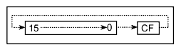
Figure 5: The bit logic for the RR instruction.
|
| DD FC |
RR IX |
4 (2,2) |
{IX,CF} = {CF,IX} |
| FD FC |
RR IY |
4 (2,2) |
{IY,CF} = {CF,IY} |
Description
Rotates to the right with the C flag the data in IX or IY. Bit 0 moves to the C flag, bits 1 through 15 move to
the next lowest-order bit position, and the C flag moves to bit 15. See Figure 5 on page 123.
|
----
CB 1F
CB 18
CB 19
CB 1A
CB 1B
CB 1C
CB 1D |
RR r
RR A
RR B
RR C
RR D
RR E
RR H
RR L |
4 (2,2)
4 (2,2)
4 (2,2)
4 (2,2)
4 (2,2)
4 (2,2)
4 (2,2)
4 (2,2) |
{r,CF} = {CF,r}
{A,CF} = {CF,A}
{B,CF} = {CF,B}
{C,CF} = {CF,C}
{D,CF} = {CF,D}
{E,CF} = {CF,E}
{H,CF} = {CF,H}
{L,CF} = {CF,L} |
Description
Rotates to the right with the C flag the data in register r (any of the registers A, B, C, D, E, H, or L). Bit 0
moves to the C flag, bits 1 through 7 move to the next lowest-order bit position, and the C flag moves to bit 7.
See Figure 4 on page 122.
Description
Rotates to the right with the C flag the data in A. Bit 0 moves to the C flag, bits 1 through 7 move to the next
lowest-order bit position, and the C flag moves to bit 7. See Figure 4 on page 122.
RRC (HL)
RRC (IX+d)
RRC (IY+d)
|
|
|
| CB 0E |
RRC (HL) |
10 (2,2,1,2,3) |
(HL) = {(HL)[0],(HL)[7,1]};
CF = (HL)[0] |
| DD CB d 0E |
RRC (IX+d) |
13 (2,2,2,2,2,3) |
(IX + d) = {(IX + d)[0],
(IX + d)[7,1]};
CF = (IX + d)[0] |
| FD CB d 0E |
RRC (IY+d) |
13 (2,2,2,2,2,3) |
(IY + d) = {(IY + d)[0],
(IY + d)[7,1]};
CF = (IY + d)[0] |
Description
Rotates to the right the data whose address is:
- the data in HL, or
- the sum of the data in IX and a displacement d, or
- the sum of the data in IY and a displacement d.
Each bit in the register moves to the next lowest-order bit position (bit 7 moves to bit 6, etc.) while bit 0
moves to both bit 7 and the C flag. See figure below.
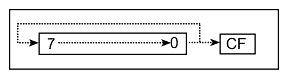
Figure 6: The bit logic of the RRC instruction.
|
----
CB 0F
CB 08
CB 09
CB 0A
CB 0B
CB 0C
CB 0D |
RRC r
RRC A
RRC B
RRC C
RRC D
RRC E
RRC H
RRC L |
4 (2,2)
4 (2,2)
4 (2,2)
4 (2,2)
4 (2,2)
4 (2,2)
4 (2,2)
4 (2,2) |
r = {r[0],r[7,1]}; CF = r[0]
A = {A[0],A[7,1]}; CF = A[0]
B = {B[0],B[7,1]}; CF = B[0]
C = {C[0],C[7,1]}; CF = C[0]
D = {D[0],D[7,1]}; CF = D[0]
E = {E[0],E[7,1]}; CF = E[0]
H = {H[0],H[7,1]}; CF = H[0]
L = {L[0],L[7,1]}; CF = L[0] |
Description
Rotates to the right the data in r (any of the registers A, B, C, D, E, H, or L). Each bit in the register moves to
the next lowest-order bit position (bit 7 moves to bit 6, etc.) while bit 0 moves to both bit 7 and the C flag. See
Figure 6 on page 127.
|
| 0F |
RRCA |
2 |
A = {A[0],A[7,1]}; CF = A[0] |
Description
Rotates to the right the data in A. Each bit in the register moves to the next lowest-order bit position (bit 7
moves to bit 6, etc.) while bit 0 moves to both bit 7 and the C flag. See Figure 6 on page 127.
|
----
D7
DF
E7
EF
FF |
RST v
RST 10
RST 18
RST 20
RST 28
RST 38 |
8 (2,2,2,2)
8 (2,2,2,2)
8 (2,2,2,2)
8 (2,2,2,2)
8 (2,2,2,2)
8 (2,2,2,2) |
(SP - 1) = PC(high); (SP - 2) = PC(low);
SP = SP - 2; PC = Restart Address
{IIR, 0x20}
{IIR, 0x30}
{IIR, 0x40}
{IIR, 0x50}
{IIR, 0x70} |
Description
Pushes the current Program Counter, PC, onto the stack and then resets the PC to the interrupt vector address
represented by IIR:v, where IIR is the address of the interrupt table and v is the offset into the table. The
address of the vector table can be read and set by the instructions LD A,IIR and LD IIR,A respectively, where
A is the upper nibble of the 16 bit vector table address. The vector table is always on a 100h boundary.
The push is accomplished by first loading the high-order byte of the PC into the memory location with the
address 1 less than the number in the Stack Pointer, SP. Then the low-order byte of the PC is loaded into the
memory location with the address two less than the number in SP. The value in SP is then decremented twice.
The PC is reset by loading it with the address to reset to v (any of the addresses 0020, 0030, 0040, 0050, or
0070).
SBC A,(HL)
SBC (IX+d)
SBC (IY+d)
|
|
|
| 9E |
SBC A,(HL) |
5 (2,1,2) |
A = A - (HL) - CF |
| DD 9E d |
SBC (IX+d) |
9 (2,2,2,1,2) |
A = A - (IX + d) - CF |
| FD 9E d |
SBC (IY+d) |
9 (2,2,2,1,2) |
A = A - (IY + d) - CF |
Description
Subtracts the C flag and the data whose address is:
- the data in HL, or
- the sum of the data in IX and a displacement d, or
- the sum of the data in IY and a displacement d
from the data in A. The result is stored in A.
These operations output an inverted carry:
- The C flag is set if A is less than the data being subtracted from it.
- The C flag is cleared if A is greater than the data being subtracted from it.
- The C flag is unchaged if A is equal to the data being subracted from it.
|
| DE n |
SBC A,n |
4 (2,2) |
A = A - n - CF |
----
9F
98
99
9A
9B
9C
9D |
SBC A,r
SBC A,A
SBC A,B
SBC A,C
SBC A,D
SBC A,E
SBC A,H
SBC A,L |
2
2
2
2
2
2
2
2 |
A = A - r - CF
A = A - A - CF
A = A - B - CF
A = A - C - CF
A = A - D - CF
A = A - E - CF
A = A - H - CF
A = A - L - CF |
Description
-
SBC A,n: Subtracts the C flag and the 8-bit constant n from the data in A.
-
SBC A,r: Subtracts the C flag and the data in r (any of the registers A, B, C, D, E, H, or L) from the data in A.
The difference is stored in A.
These operations output an inverted carry:
- The C flag is set if A is less than the data being subtracted from it.
- The C flag is cleared if A is greater than the data being subtracted from it.
- The C flag is unchaged if A is equal to the data being subracted from it.
|
----
ED 42
ED 52
ED 62
ED 72 |
SBC HL,ss
SBC HL,BC
SBC HL,DE
SBC HL,HL
SBC HL,SP |
4 (2,2)
4 (2,2)
4 (2,2)
4 (2,2)
4 (2,2) |
HL = HL - ss - CF
HL = HL - BC - CF
HL = HL - DE - CF
HL = HL - HL - CF
HL = HL - SP - CF |
Description
Subtracts the C flag and the data in ss (any of BC, DE, HL, or SP) from the data in HL. The difference is
stored in HL.
These operations output an inverted carry:
- The C flag is set if A is less than the data being subtracted from it.
- The C flag is cleared if A is greater than the data being subtracted from it.
- The C flag is unchaged if A is equal to the data being subracted from it.
Description
Sets the C flag.
SET b,(HL)
SET b,(IX+d)
SET b,(IY+d)
|
|
|
CB C6
CB CE
CB D6
CB DE
CB E6
CB EE
CB F6
CB FE |
SET b,(HL)
SET bit 0,(HL)
SET bit 1,(HL)
SET bit 2,(HL)
SET bit 3,(HL)
SET bit 4,(HL)
SET bit 5,(HL)
SET bit 6,(HL)
SET bit 7,(HL) |
10* 10* 10* 10* 10* 10* 10* 10* 10* |
(HL) = (HL) | bit
(HL) = (HL) | bit 0
(HL) = (HL) | bit 1
(HL) = (HL) | bit 2
(HL) = (HL) | bit 3
(HL) = (HL) | bit 4
(HL) = (HL) | bit 5
(HL) = (HL) | bit 6
(HL) = (HL) | bit 7 |
DD CB d C6
DD CB d CE
DD CB d D6
DD CB d DE
DD CB d E6
DD CB d EE
DD CB d F6
DD CB d FE |
SET b,(IX+d)
SET bit 0,(IX+d)
SET bit 1,(IX+d)
SET bit 2,(IX+d)
SET bit 3,(IX+d)
SET bit 4,(IX+d)
SET bit 5,(IX+d)
SET bit 6,(IX+d)
SET bit 7,(IX+d) |
13** 13** 13** 13** 13** 13** 13** 13** 13** |
(IX + d) = (IX + d) | bit
(IX + d) = (IX + d) | bit 0
(IX + d) = (IX + d) | bit 1
(IX + d) = (IX + d) | bit 2
(IX + d) = (IX + d) | bit 3
(IX + d) = (IX + d) | bit 4
(IX + d) = (IX + d) | bit 5
(IX + d) = (IX + d) | bit 6
(IX + d) = (IX + d) | bit 7 |
FD CB d C6
FD CB d CE
FD CB d D6
FD CB d DE
FD CB d E6
FD CB d EE
FD CB d F6
FD CB d FE |
SET b,(IY+d)
SET bit 0,(IY+d)
SET bit 1,(IY+d)
SET bit 2,(IY+d)
SET bit 3,(IY+d)
SET bit 4,(IY+d)
SET bit 5,(IY+d)
SET bit 6,(IY+d)
SET bit 7,(IY+d) |
13** 13** 13** 13** 13** 13** 13** 13** 13** |
(IY + d) = (IY + d) | bit
(IY + d) = (IY + d) | bit 0
(IY + d) = (IY + d) | bit 1
(IY + d) = (IY + d) | bit 2
(IY + d) = (IY + d) | bit 3
(IY + d) = (IY + d) | bit 4
(IY + d) = (IY + d) | bit 5
(IY + d) = (IY + d) | bit 6
(IY + d) = (IY + d) | bit 7 |
Clocking: *10 (2,2,1,2,3) **13 (2,2,2,2,2,3) |
Description
Sets bit b (any of the bits 0, 1, 2, 3, 4, 5, 6, or 7) of the byte whose address is
- the data in HL, or
- the sum of the data in IX and a displacement d, or
- the sum of the data in IY and a displacement d.
|
|
SET b,r |
4 (2,2) |
r = r | bit |
Description
Sets bit b (any of the bits 0, 1, 2, 3, 4, 5, 6, or 7) of the data in r (any of the registers A, B, C, D, E, H, or L).
SETUSR Rabbit 3000A Instruction
|
|
|
| ED 6F |
SETUSR |
4 (2,2) |
SU={SU[5:0],0x01} |
Description
The System/User Mode Register, SU, is an 8 bit register that forms a stack of the current processor mode and
the previous 3 modes. SETUSR shifts the contents of SU 2 bits to the left, then sets bit 1 to 0 and bit 0 to 1,
signifying user mode.
This instruction is privileged and only implemented for the Rabbit 3000A.
SLA (HL)
SLA (IX+d)
SLA (IY+d)
|
|
|
| CB 26 |
SLA (HL) |
10* |
(HL) = {(HL)[6,0],0}; CF = (HL)[7] |
| DD CB d 26 |
SLA (IX+d) |
13** |
(IX + d) = {(IX + d)[6,0],0};
CF = (IX + d)[7] |
| FD CB d 26 |
SLA (IY+d) |
13** |
(IY + d) = {(IY + d)[6,0],0};
CF = (IY + d)[7] |
Clocking: *10 (2,2,1,2,3) **13 (2,2,2,2,2,3) |
Description
Arithmetically shifts to the left the bits of the data whose address is
- the data in HL, or
- the sum of the data in IX and a displacement d, or
- the sum of the data in IY and a displacement d.
Bits 0 through 6 are each shifted to the next highest-order bit position (bit 0 moves to bit 1, etc.). Bit 7 is
shifted to the C flag. Bit 0 is reset. See figure below.
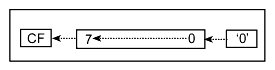
Figure 7: The bit logic of the SLA instruction.
|
----
CB 27
CB 20
CB 21
CB 22
CB 23
CB 24
CB 25 |
SLA r
SLA A
SLA B
SLA C
SLA D
SLA E
SLA H
SLA L |
4 (2,2)
4 (2,2)
4 (2,2)
4 (2,2)
4 (2,2)
4 (2,2)
4 (2,2)
4 (2,2) |
r = {r[6,0],0}; CF = r[7]
A = {A[6,0],0}; CF = A[7]
B = {B[6,0],0}; CF = B[7]
C = {C[6,0],0}; CF = C[7]
D = {D[6,0],0}; CF = D[7]
E = {E[6,0],0}; CF = E[7]
H = {H[6,0],0}; CF = H[7]
L = {L[6,0],0}; CF = L[7] |
Description
Arithmetically shifts to the left the bits of the data in register r (any of A, B, C, D, E, H, or L). Bits 0 through
6 are each shifted to the next highest-order bit position (bit 0 moves to bit 1, etc.). Bit 7 is shifted to the C flag.
Bit 0 is reset. See Figure 7 on page 138.
SRA (HL)
SRA (IX+d)
SRA (IY+d)
|
|
|
| CB 2E |
SRA (HL) |
10* |
(HL) = {(HL)[7],(HL)[7,1]};
CF = (HL)[0] |
| DD CB d 2E |
SRA (IX+d) |
13** |
(IX + d) = {(IX + d)[7],(IX + d)[7,1]}; CF = (IX + d)[0] |
| FD CB d 2E |
SRA (IY+d) |
13** |
(IY +d) = {(IY + d)[7],(IY + d)[7,1]}; CF = (IY + d)[0] |
Clocking: *10 (2,2,1,2,3) **13 (2,2,2,2,2,3) |
Description
Arithmetically shifts to the right the bits in the data whose address is
- the data in HL, or
- the sum of the data in IX and a displacement d, or
- the sum of the data in IY and a displacement d.
Bits 7 through 1 are shifted to the next lowest-order bit position (bit 7 is shifted to bit 6, etc.). Bit 7 is also copied
to itself. Bit 0 is shifted to the C flag. See figure below.
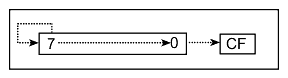
Figure 8: The bit logic of the SRA instruction.
|
----
CB 2F
CB 28
CB 29
CB 2A
CB 2B
CB 2C
CB 2D |
SRA r
SRA A
SRA B
SRA C
SRA D
SRA E
SRA H
SRA L |
4 (2,2)
4 (2,2)
4 (2,2)
4 (2,2)
4 (2,2)
4 (2,2)
4 (2,2)
4 (2,2) |
r = {r[7],r[7,1]}; CF = r[0]
A = {A[7],A[7,1]}; CF = A[0]
B = {B[7],B[7,1]}; CF = B[0]
C = {C[7],C[7,1]}; CF = C[0]
D = {D[7],D[7,1]}; CF = D[0]
E = {E[7],E[7,1]}; CF = E[0]
H = {H[7],H[7,1]}; CF = H[0]
L = {L[7],L[7,1]}; CF = L[0] |
Description
Arithmetically shifts to the right the bits in r (any of the registers A, B, C, D, E, H, or L). Bits 7 through 1 are
shifted to the next lowest-order bit position (bit 7 is shifted to bit 6, etc.). Bit 7 is also copied to itself. Bit 0 is
shifted to the C flag. See Figure 8 on page 140.
SRL (HL)
SRL (IX+d)
SRL (IY+d)
|
|
|
| CB 3E |
SRL (HL) |
10* |
(HL) = {0,(HL)[7,1]}; CF = (HL)[0] |
| DD CB d 3E |
SRL (IX+d) |
13** |
(IX + d) = {0,(IX + d)[7,1]};
CF = (IX + d)[0] |
| FD CB d 3E |
SRL (IY+d) |
13** |
(IY + d) = {0,(IY + d)[7,1]};
CF = (IY + d)[0] |
Clocking: *10 (2,2,1,2,3) **13 (2,2,2,2,2,3) |
Description
Logically shifts to the right the bits of the data whose address is
- the data in HL, or
- the sum of the data in IX and a displacement d, or
- the sum of the data in IY and a displacement d.
Each bit is shifted to the next lowest-order bit position (Bit 7 shifts to bit 6, etc.) Bit 0 shift to the C flag. Bit 7
is reset. See figure below.
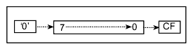
Figure 9: The bit logic of the SRL instruction.
|
----
CB 3F
CB 38
CB 39
CB 3A
CB 3B
CB 3C
CB 3D |
SRL r
SRL A
SRL B
SRL C
SRL D
SRL E
SRL H
SRL L |
4 (2,2)
4 (2,2)
4 (2,2)
4 (2,2)
4 (2,2)
4 (2,2)
4 (2,2)
4 (2,2) |
r = {0,r[7,1]}; CF = r[0]
A = {0,A[7,1]}; CF = A[0]
B = {0,B[7,1]}; CF = B[0]
C = {0,C[7,1]}; CF = C[0]
D = {0,D[7,1]}; CF = D[0]
E = {0,E[7,1]}; CF = E[0]
H = {0,H[7,1]}; CF = H[0]
L = {0,L[7,1]}; CF = L[0] |
Description
Logically shifts to the right the bits in r (any of the registers A, B, C, D, E, H, or L). Each bit is shifted to the
next lowest-order bit position (Bit 7 shifts to bit 6, etc.) Bit 0 shift to the C flag. Bit 7 is reset. See Figure 9 on
page 142.
SUB (HL)
SUB (IX+d)
SUB (IY+d)
|
|
|
| 96 |
SUB (HL) |
5 (2,1,2) |
A = A - (HL) |
| DD 96 d |
SUB (IX+d) |
9 (2,2,2,1,2) |
A = A - (IX + d) |
| FD 96 d |
SUB (IY+d) |
9 (2,2,2,1,2) |
A = A - (IY + d) |
Description
Subtracts from the data in A the data whose address is
- the data in HL, or
- the sum of the data in IX and a displacement d, or
- the sum of the data in IY and a displacement d.
The result is stored in A.
|
| D6 n |
SUB n |
4 (2,2) |
A = A - n |
Description
Subtracts from the data in A the 8-bit constant n. The result is stored in A.
|
----
97
90
91
92
93
94
95 |
SUB r
SUB A
SUB B
SUB C
SUB D
SUB E
SUB H
SUB L |
2
2
2
2
2
2
2
2 |
A = A - r
A = A - A
A = A - B
A = A - C
A = A - D
A = A - E
A = A - H
A = A - L |
Description
Subtracts from the data in A the data in r (any of the registers A, B, C, D, E, H, or L). The result is stored in A.
SURES Rabbit 3000A Instruction
|
|
|
| ED 7D |
SURES |
4 (2,2) |
SU = {SU[1:0],SU[7:2]} |
Description
The SURES instruction rotates the contents of the System/User Mode Register SU 2 bits to the right, replacing
the current processor mode with the previous mode.
This instruction is privileged and only implemented for the Rabbit 3000A.
SYSCALL Rabbit 3000A Instruction
|
|
|
| ED 75 |
SYSCALL |
10 (2,2,3,3) |
SP = SP-2; PC = {R,v}
where v = SYSCALL offset |
Description
Pushes the current PC onto the stack and then resets the PC to the interrupt vector address represented by
IIR:0x60, where IIR is the address of the interrupt table and 0x60 is the offset into the table. The address of
the vector table can be read and set by the instructions LD A,IIR and LD IIR,A respectively, where A is
the upper nibble of the 16 bit vector table address. The vector table is always on a 100h boundary.
The push is accomplished by first loading the high-order byte of the PC into the memory location with the
address 1 less than the number in SP. Then the low-order byte of the PC is loaded into the memory location
with the address two less than the number in SP. The value in SP is then decremented twice.
This instruction is implemented in the Rabbit 3000A.
UMA
UMS   Rabbit 3000A Instructions
|
|
|
| ED C0 |
UMA |
8+8i (2,2,2, (2,2,3,1)i,2) |
[CY:DE':(HL)} =
(IX) + [(IY)*DE+DE'+CY];
BC = BC - 1; IX = IX + 1;
IY = IY + 1; HL = HL + 1;
repeat while BC != 0 |
| ED C8 |
UMS |
8+8i (2,2,2, (2,2,3,1)i,2) |
[CY:DE':(HL)} =
(IX) - [(IY)*DE+DE'+CY];
BC = BC - 1; IX = IX + 1;
IY = IY + 1; HL = HL + 1;
repeat while BC != 0
|
Description
While the data in the BC does not equal 0, then:
- the data at the address in IY is multiplied by the data in DE;
- the data in alternate register DE' is added to that value;
- the C flag is added to that value; and
- this value is added to the data at the address in IX (for UMA) or
this value is subtracted from the data at the address in IX (for UMS).
This results in a 24-bit value. The lowest eight bits of this value are stored memory at the address in HL, and
the upper 16 bits are stored in the alternate register DE'. If The data in IX, IY, and HL are then incremented,
and the data in BC is decremented. The instruction then repeats until BC equals zero. Interrupts can occur
between different repeats, but not within an iteration.
These instructions are implemented in the Rabbit 3000A.
XOR (HL)
XOR (IX+d)
XOR (IY+d)
|
|
|
| AE |
XOR (HL) |
5 (2,1,2) |
A = [A & ~(HL)] | [~A & (HL)] |
| DD AE d |
XOR (IX+d) |
9 (2,2,2,1,2) |
A = [A & ~(IX + d)] |
[~A & (IX + d)] |
| FD AE d |
XOR (IY+d) |
9 (2,2,2,1,2) |
A = [A & ~(IY + d)] |
[~A & (IY + d)] |
Description
Performs an exclusive OR operation between the data in A and the data whose address is:
- the data in HL, or
- the sum of the data in IX and a displacement d, or
- the sum of the data in IY and a displacement d.
The corresponding bits of each byte are compared (i.e., bit 0 of both bytes are compared, bit 1 of both bytes
are compared, etc.). The associated bit in the result byte is set if and only if one of the two compared bits is
set. The result is stored in A.
Example
If HL contains 0x4000 and the memory location 0x4000 contains the byte 1001 0101 and A contains the byte
0101 0011 then the execution of the instruction
XOR (HL)
would result in the byte in A becoming 1100 0110.
|
| EE n |
XOR n |
4 (2,2) |
A = [A & ~n] | [~A & n] |
Description
Performs an exclusive OR operation between the byte in A and the 8-bit constant n. The corresponding bits of
each byte are compared (i.e., bit 0 of both bytes are compared, the bit 1 of both bytes are compared, etc.). The
associated bit in the result byte is set if and only if one of the two compared bits is set. The result is stored in
A.
|
----
AF
A8
A9
AA
AB
AC
AD |
XOR r
XOR A
XOR B
XOR C
XOR D
XOR E
XOR H
XOR L |
2
2
2
2
2
2
2
2 |
A = [A & ~r] | [~A & r]
A = [A & ~A] | [~A & A]
A = [A & ~B] | [~A & B]
A = [A & ~C] | [~A & C]
A = [A & ~D] | [~A & D]
A = [A & ~E] | [~A & E]
A = [A & ~H] | [~A & H]
A = [A & ~L] | [~A & L] |
Description
Performs an exclusive OR operation between the byte in A and r (any of the registers A, B, C, D, E, H, or L).
The corresponding bits of each byte are compared (i.e., bit 0 of both bytes are compared, bit 1 of both bytes
are compared, etc.). The associated bit in the result byte is set if and only if one of the two compared bits is
set. The result is stored in A.