| Rabbit 2000™ Microprocessor User's Manual |
8. Memory Mapping and Interface
See Section 3.2, "Memory Mapping," for a discussion of the Rabbit memory mapping.
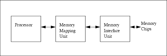
Figure 8-1 shows an overview of the Rabbit memory mapping. The task of the memory mapping unit is to accept 16-bit addresses and translate them to 20-bit addresses. The memory interface unit accepts the 20-bit addresses and generates control signals applied directly to the memory chips.
8.1 Memory-Mapping Unit
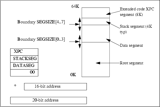
The 64K 16-bit address space accessed by processor instructions is divided into segments. Each segment has a length that is a multiple of 4K. Except for the extended code segment, the segments have adjustable sizes and some segments can be reduced to zero size and thus vanish from the memory map.
The four segments are shown in the example in Figure 8-2. The segment size register (SEGSIZE) determines the boundaries marked in the diagram. The extended code segment always occupies the addresses 0E000h-0FFFFh. The stack segment stretches from the address specified by the upper 4 bits of the SEGSIZE register to 0DFFFh. For example, if the upper 4 bits of SEGSIZE are 0Dh, then the stack segment will occupy 0D000h-0DFFFh, or 4K. If the upper 4 bits of SEGSIZE are greater than or equal to 0Eh, the stack segment vanishes. If these bits are set to zero, the two segments below the stack segment will vanish.
The lower 4 bits of SEGSIZE determine the lower boundary shown in the figure. If this boundary is equal to the upper boundary or greater than 0Eh, the data segment will vanish. If this segment is placed at zero the code segment will vanish.
The memory management unit accepts a 16-bit address from the processor and translates it into a 20-bit address. The procedure to do this works as follows.
- It is determined which segment the 16-bit address belongs to by inspecting the upper 4 bits of the address. Every address must belong to one of the possible 4 segments.
- Each segment has an 8-bit segment register. The 8-bit segment register is added to the upper 4 bits of the 16-bit address to create a 20-bit address. Wraparound occurs if the addition would result in an address that does not fit in 20 bits.
Table 8-2. Segment Size Register SEGSIZE = 13h Boundary address stack segment. Boundary address data segment. 8.2 Memory Interface Unit
The 20-bit memory addresses generated by the memory-mapping unit feed into the memory interface unit. The memory interface unit has a separate write-only control register (see Table 8-3) for each 256K quadrant of the 1M physical memory. This control register specifies how memory access requests to that quadrant are to be dispatched to the memory chips connected to the Rabbit. There are three separate chip select output lines (/CS0, /CS1, and /CS2) that can be used to select one of three different memory chips. A field in the control register determines which chip select is selected for memory accesses to the quadrant. The same chip select line may be accessed in more than one quadrant. For example, if a 512K RAM is installed and is selected by /CS1, it would be appropriate to use /CS1 for accesses to the 3rd and 4th quadrants, thus mapping the RAM chip to addresses 80000h to 0FFFFFh.
8.3 Memory Bank Control Registers
Table 8-3 describes the operation of the four memory bank control registers. The registers are write-only. Each register controls one quadrant in the 1M address space.
- Bits 7,6--The number of wait states used in access to this quadrant. Without wait states, read requires 2 clocks and write requires 3 clocks. The wait state adds to these numbers. Wait states should only be used for memory data accesses (RAM or data flash), not for memory from which instructions are executed (code memory).
- Bits 5, 4--These bits allow the upper address lines to be inverted. This inversion occurs after the logic that selects the bank register, so setting these lines has no effect on which bank register is used. The inversion may be used to install a 1M memory chip in the space normally allocated to a 256K chip. The larger memory can then be accessed as 4 pages of 256K each. There is no effect outside the quadrant that the memory bank control register is controlling.
- Bit 3--Inhibits the write pulse to memory accessed in this quadrant. Useful for protecting flash memory from an inadvertent write pulse, which will not actually write to the flash because it is protected by lock codes, but will temporarily disable the flash memory and crash the system if the memory is used for code.
- Bit 2--Selects which set of the two lines /OEx and /WEx will be driven for memory accesses in this quadrant.
- Bits 1,0--Determines which of the three chip select lines will be driven for memory accesses to this quadrant.
- All bits of the control register are initialized to zero on reset.
8.3.1 Optional A16, A19 Inversions by Segment (/CS1 Enable)
The inversion of A19 or A16 controlled by the read/write MMIDR register is used to redirect mapping of the root segment and the data segment by inverting certain bits when these segments are accessed. Currently there is no planned use for this functionality.
The optional enable of /CS1 is valuable for systems that are pushing the access time of battery-backed RAM. By enabling /CS1, the delay time of the switch that forces /CS1 high when power is off can be bypassed. This feature increases power consumption since the RAM is always enabled and its access is controlled normally by /OE1.
Table 8-4. MMU Instruction/Data Register (MMIDR = 010h) 000
1--force /CS1 to be always enabled
These bits must always be 0
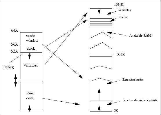
8.4 Allocation of Extended Code and Data
The Dynamic C compiler compiles code to root code space or to extended code space. Root code starts in low memory and compiles upward.
Allocation of extended code starts above the root code and data. Allocation normally continues to the end of the flash memory.
Data variables are allocated to RAM working backwards in memory. Allocation normally starts at 52K in the 64K D space and continues. The 52K space must be shared with the root code and data, and is allocated upward from zero.
Dynamic C also supports extended data constants. These are mixed in with the extended code in flash.
8.5 How Compiler Compiles to Memory
The compiler actually generates code for root code and constants and extended code and extended constants. It allocates space for data variables, but does not generate data bits to be stored in memory.
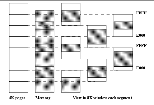
In any but the smallest programs, most of the code is compiled to extended memory. This code executes in the 8K window from E000 to FFFF. This 8K window uses paged access. Instructions that use 16-bit addressing can jump within the page and also outside of the page to the remainder of the 64K space. Special instructions, particularly long call, long jump and long return, are used to access code outside of the 8K window. When one of these transfer of control instructions is executed, both the address and the view through the 8K window or page are changed. This allows transfer to any instruction in the 1M memory space. The 8-bit XPC register controls which of the 256 4K pages the 8K window aligns with. The 16-bit PC controls the address of the instruction, usually in the region E000 to FFFF. The advantage of paged access is that most instructions continue to use 16-bit addressing. Only when an out-of-range transfer of control is made does a 20-bit transfer of control need to be made. The beauty of having a 4K minimum step in page alignment while the size of the page is 8K is that code can be compiled continuously without gaps caused by change of page. When the page is moved by 4K, the previous end of code is still visible in the window, provided that the midpoint of the page was crossed before moving the page alignment.
As the compiler compiles code in the extended code window, it checks at opportune times to see if the code has passed the midpoint of the window or F000. When the code passes F000, the compiler slides the window down by 4K so that the code at F000+x becomes resident at E000+x. This results in the code being divided into segments that are typically 4K long, but which can very short or as long as 8K. Transfer of control can be accomplished within each segment by 16-bit addressing; 20-bit addressing is required between segments.
| Rabbit Semiconductor http://www.rabbitsemiconductor.com Voice: (530) 757-8400 FAX: (530) 757-8402 sales@rabbitsemiconductor.com |