| Rabbit 2000™ Microprocessor User's Manual |
9. Parallel Ports
The Rabbit has five 8-bit parallel ports designated A, B, C, D and E. The pins used for the parallel ports are also shared with numerous other functions as shown in Table 5-2. The important properties of the ports are summarized below.
- Port A—Shared with the slave port data interface.
- Port B—Shared with control lines for slave port and clock I/O for clocked serial mode option for serial ports A and B.
- Port C—Shared with serial port serial data I/O.
- Port D—4 bits shared with alternate I/O pins for serial ports A and B. 4 bits not shared. Port D has the ability to configure its outputs as open drain outputs. Port D has output preload registers that can be clocked into the output registers under timer control for pulse generation. Port D bits 0-3 have a higher current drive capability.
- Port E—All bits of Port E can be configured as I/O strobes. 4 bits of port E can be used as external interrupt inputs. One bit of port E is shared with the slave port chip select. Port E has output preload registers that can be clocked into the output registers under timer control for pulse generation.
9.1 Parallel Port A
Parallel Port A has a single read/write register:
Table 9-1. Parallel Port A Data Register PADR (adr = 030h) R/W 8-bit Data Value
This register should not be used if the slave port is enabled.
The slave port control register is used to control whether Parallel Port A is an output or an input. To make the port an input, store 080h in the SPCR (slave port control register). To make the port an output, store 084h in SPCR. Parallel Port A is set up as an input port on reset.
When the port is read, the value read reflects the voltages on the pins, "1" for high and "0" for low. This could be different than the value stored in the output register if the pin is forced to a different state by an external voltage.
9.2 Parallel Port B
Parallel Port B, shown in Table 9-2, has six inputs and two outputs when used exclusively as a parallel port.
Table 9-2. Parallel Port B Data Register PBDR (adr = 040h) Read
Echo drive
Echo drive
PB5 in
PB4 in
PB3 in
PB2 in
PB1 in
PB0 in
Write
PB7
PB6
x
x
x
x
x
x
When the slave port is enabled, parallel port lines PB2-PB7 are assigned to various slave port functions. However, it is still possible to read PB0-PB5 using the Port B data register even when lines PB2-PB7 are used for the slave port. It is also possible to read the signal driving PB6 and PB7 (this signal is on the signaling lines from the slave port logic).
Regardless of whether the slave port is enabled, PB0 reflects the input of the pin unless serial port B has its internal clock enabled, which causes this line to be driven by the serial port clock. PB1 reflects the input of the pin unless serial port A has its internal clock enabled.
On reset the output bits 6 and 7 are reset and the value output on pins PB6 and PB7 (package pins 99, 100) will also be low.
9.3 Parallel Port C
Parallel port C, shown in Table 9-3, has four inputs and four outputs. The even-numbered ports, PC0, PC2, PC4, and PC6, are outputs. The odd-numbered ports, PC1, PC3, PC5, and PC7, are inputs. When the data register is read, bits 1,3,5,7 return the value of the voltage on the pin. Bits 0,2,4,6 return the value of the signal driving the output buffers. The signal driving the output buffers and the value of the output pin are normally the same. Either the Port C data register is driving these pins or one of the serial port transmit lines is driving the pin. The bits set in the PCFR Parallel Port C Function Register identify whether the data register or the serial port transmit lines were driving the pins.
Parallel port C shares its pins with the four serial ports. The parallel port input pins may also serve as serial port inputs. (Serial ports A and B can alternately use bits 7 and 5 respectively in Port D as inputs, and the source of the serial port inputs for these serial ports depends on the setup of the corresponding serial port control register.) When serving as serial inputs, the data lines can still be read from the parallel port C data register. The parallel port outputs can be selected to be serial port outputs by storing bits in the corresponding positions of the Port C Function register (PCFR). When a parallel port output pin is selected to be a serial port output, the value stored in the data register is ignored. On reset the active (even-numbered) function register bits and data register bits are zeroed. This causes the port to output zeros on the four output bits.
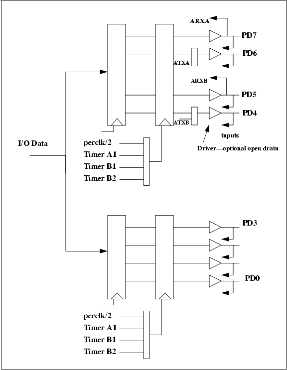
9.4 Parallel Port D
Parallel port D, shown in Figure 9-1, has eight pins that can programmed individually to be inputs and outputs. When programmed as outputs, the pins can be individually selected to be open-drain outputs or standard outputs. Port D pins can be addressed by bit if desired. The output registers are cascaded and timer-controlled, making it possible to generate precise timing pulses. In addition, port D outputs have a higher drive capability. Port D bits 4 and 5 can be used as alternate bits for serial port B, and bits 6 and 7 can be used as alternate bits for serial port A. Alternate serial port bit assignments make it possible for the same serial port to connect to different communications lines that are not operating at the same time.
On reset, the data direction register is zeroed, making all pins inputs. In addition bits in the control register are zeroed (bits 0,1,4,5) to ensure that data is clocked into the output registers when loaded. All other registers associated with port D are not initialized on reset.
The following registers are described in Table 9-4 and in Table 9-5.
- PDDR—Parallel port D data register. Read/Write.
- PDDDR—Parallel port D data direction register. A "1" makes the corresponding pin an output. Write only.
- PDDCR—Parallel port D drive control register. A "1" makes the corresponding pin an open-drain output if that pin is set up for output. Write only.
- PDFR—Parallel port D function control register. This port may be used to make port positions 4 and 6 be serial port outputs. Write only.
- PDBxR—These eight registers may be used to set outputs on individual port positions.
- PDCR—Parallel port D control register. This register is used to control the clocking of the upper and lower nibble of the final output register of the port. On reset, bits 0, 1, 4, and 5 are reset to zero.
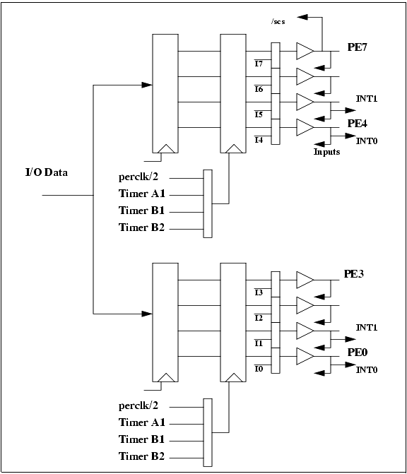
9.5 Parallel Port E
Parallel port E, shown in Figure 9-2, has eight I/O pins that can be individually programmed as inputs or outputs. Port E has a higher drive than most of the other ports. PE7 is used as the slave port chip select when the slave port is enabled. Each of the port E outputs can be configured as an I/O strobe. In addition, four of the port E lines can be used as interrupt request inputs. The output registers are cascaded and timer-controlled, making it possible to generate precise timing pulses.
The following registers are described in Table 9-6 and in Table 9-7.
- PEDR—Port E data register. Reads value at pins. Writes to port E preload register.
- PEDDR—Port E data direction register. Set to "1" to make corresponding pin an output. This register is zeroed on reset.
- PEFR—Port E function register. Set bit to "1" to make corresponding output an I/O strobe. The nature of the I/O strobe is controlled by the I/O bank control registers (IBxCR). The data direction must be set to output for the I/O strobe to work.
- PEBxR—These are individual registers to set individual output bits on or off.
- PECR—Parallel port E control register. This register is used to control the clocking of the upper and lower nibble of the final output register of the port. On reset, bits 0, 1, 4, and 5 are reset to zero.
| Rabbit Semiconductor http://www.rabbitsemiconductor.com Voice: (530) 757-8400 FAX: (530) 757-8402 sales@rabbitsemiconductor.com |