
User's Manual
|
| RabbitCore RCM4500W User's Manual |
4. Hardware Reference
Chapter 4 describes the hardware components and principal hardware subsystems of the RCM4510W. Appendix A, "RCM4510W Specifications," provides complete physical and electrical specifications.
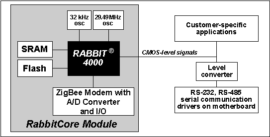
Figure 6 shows the Rabbit-based subsystems designed into the RCM4510W.
4.1 RCM4510W Digital Inputs and Outputs
Figure 7 shows the RCM4510W pinouts for headers J1 and J4.
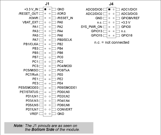
Headers J1 is a standard 2 × 25 IDC header with a nominal 1.27 mm pitch, and header J4 is a standard 2 × 7 IDC header with a nominal 2 mm pitch.
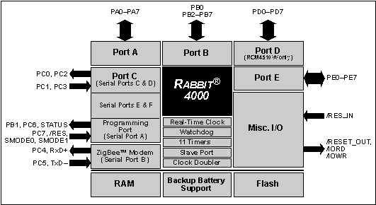
Figure 8 shows the use of the Rabbit 4000 microprocessor ports in the RCM4510W modules.
The ports on the Rabbit 4000 microprocessor used in the RCM4510W are configurable, and so the factory defaults can be reconfigured. Table 2 lists the Rabbit 4000 factory defaults and the alternate configurations.
4.1.1 Memory I/O Interface
The Rabbit 4000 address lines (A0–A19) and all the data lines (D0–D7) are routed internally to the onboard flash memory and SRAM chips. I/0 write (/IOWR) and I/0 read (/IORD) are available for interfacing to external devices, and are also used by the RCM4510W.
Parallel Port A can also be used as an external I/O data bus to isolate external I/O from the main data bus. Parallel Port B pins PB2–PB7 can also be used as an auxiliary address bus.
When using the external I/O bus for any reason, you must add the following line at the beginning of your program.
#define PORTA_AUX_IO // required to enable external I/O busSelected pins on Parallel Ports D and E as specified in Table 2 may be used for input capture, quadrature decoder, DMA, and pulse-width modulator purposes.
4.1.2 Other Inputs and Outputs
The STATUS and the two SMODE pins, SMODE0 and SMODE1, can be brought out to header J1 instead of the PE5–PE7 pins as explained in Appendix A.6.
/RESET_IN is normally associated with the programming port, but may be used as an external input to reset the Rabbit 4000 microprocessor and the RCM4510W memory. /RESET_OUT is an output from the reset circuitry that can be used to reset other peripheral devices.
4.1.3 Auxiliary I/O
Up to nine additional digital I/O, up to four of which may be configured in software as analog inputs, a +3.3 V DC power supply point and ground, and a SYS_PWR_ON line are brought out on auxiliary I/O header J4. Section 4.4 describes the use of these lines in more detail.
4.2 Serial Communication
The RCM4510W module does not have any serial driver or receiver chips directly on the board. However, a serial interface may be incorporated on the board the RCM4510W is mounted on. For example, the Prototyping Board has an RS-232 transceiver chip.
4.2.1 Serial Ports
There are six serial ports designated as Serial Ports A, B, C, D, E, and F. All six serial ports can operate in an asynchronous mode up to the baud rate of the system clock divided by 8. An asynchronous port can handle 7 or 8 data bits. A 9th bit address scheme, where an additional bit is sent to mark the first byte of a message, is also supported.
Serial Port A is normally used as a programming port, but may be used either as an asynchronous or as a clocked serial port once application development has been completed and the RCM4510W is operating in the Run Mode.
Serial Port B is shared with the RCM4510W module's asynchronous XBee RF module. Flow control for the XBee RF module is provided from the Rabbit 4000 RxD+ and TxD– Ethernet pins.
Serial Ports C and D can also be operated in the clocked serial mode. In this mode, a clock line synchronously clocks the data in or out. Either of the two communicating devices can supply the clock. Note that PD2 and PD0 provide the SCLKC and SCLKD outputs automatically when Serial Ports C and D are set up as clocked serial ports.
Serial Ports E and F can also be configured as SDLC/HDLC serial ports. The IrDA protocol is also supported in SDLC format by these two ports. Serial Ports E and F must be configured before they can be used. The sample program
IOCONFIG_SWITCHECHO.Cin the Dynamic CSAMPLES\RCM4500W\SERIALfolder shows how to configure Serial Ports E and F.Table 3 summarizes the possible parallel port pins for the serial ports and their clocks.
4.2.1.1 Using the Serial Ports
The receive lines on the RCM4510W serial ports do not have pull-up resistors. If you are using the serial ports without a receiver chip (for example, for RS-422, RS-232, or RS-485 serial communication), the absence of a pull-up resistor on the receive line will likely lead to line breaks being generated since line breaks are normally generated whenever the receive line is pulled low. If you are operating a serial port asynchronously, you can inhibit character assembly during breaks by setting bit 1 in the corresponding Serial Port Extended Register to 1. Should you need line breaks, you will have to either add a pull-up resistor on your motherboard or use a receiver that incorporates the circuits to have the output default to the nonbreak levels.
The Dynamic C
RS232.LIBlibrary requires you to define the macroRS232_NOCHARASSYINBRKto inhibit break-character assembly for all the serial ports.
#define RS232_NOCHARASSYINBRKThis macro is already defined so that it is the default behavior for the sample programs in the Dynamic C
SAMPLES\RCM4500W\SERIALfolder.4.2.2 Programming Port
The RCM4510W is programmed via the 10-pin header labeled J2. The programming port uses the Rabbit 4000's Serial Port A for communication. Dynamic C uses the programming port to download and debug programs.
Serial Port A is also used for the following operations.
- Cold-boot the Rabbit 4000 on the RCM4510W after a reset.
- Fast copy designated portions of flash memory from one Rabbit-based board (the master) to another (the slave) using the Rabbit Cloning Board.
Alternate Uses of the Programming Port
All three Serial Port A signals are available as
- a synchronous serial port
- an asynchronous serial port, with the clock line usable as a general CMOS I/O pin
The programming port may also be used as a serial port via the DIAG connector on the programming cable.
In addition to Serial Port A, the Rabbit 4000 startup-mode (SMODE0, SMODE1), STATUS, and reset pins are available on the programming port.
The two startup-mode pins determine what happens after a reset—the Rabbit 4000 is either cold-booted or the program begins executing at address 0x0000.
The status pin is used by Dynamic C to determine whether a Rabbit microprocessor is present. The status output has three different programmable functions:
- It can be driven low on the first op code fetch cycle.
- It can be driven low during an interrupt acknowledge cycle.
- It can also serve as a general-purpose output once a program has been downloaded and is running.
The reset pin is an external input that is used to reset the Rabbit 4000.
Refer to the Rabbit 4000 Microprocessor User's Manual for more information.
4.3 Programming Cable
The programming cable is used to connect the programming port of the RCM4510W to a PC serial COM port. The programming cable converts the RS-232 voltage levels used by the PC serial port to the CMOS voltage levels used by the Rabbit 4000.
When the PROG connector on the programming cable is connected to the RCM4510W programming port, programs can be downloaded and debugged over the serial interface.
The DIAG connector of the programming cable may be used on header J2 of the RCM4510W with the RCM4510W operating in the Run Mode. This allows the programming port to be used as a regular serial port.
4.3.1 Changing Between Program Mode and Run Mode
The RCM4510W is automatically in Program Mode when the PROG connector on the programming cable is attached, and is automatically in Run Mode when no programming cable is attached. When the Rabbit 4000 is reset, the operating mode is determined by the status of the SMODE pins. When the programming cable's PROG connector is attached, the SMODE pins are pulled high, placing the Rabbit 4000 in the Program Mode. When the programming cable's PROG connector is not attached, the SMODE pins are pulled low, causing the Rabbit 4000 to operate in the Run Mode.
A program "runs" in either mode, but can only be downloaded and debugged when the RCM4510W is in the Program Mode.
Refer to the Rabbit 4000 Microprocessor User's Manual for more information on the programming port.
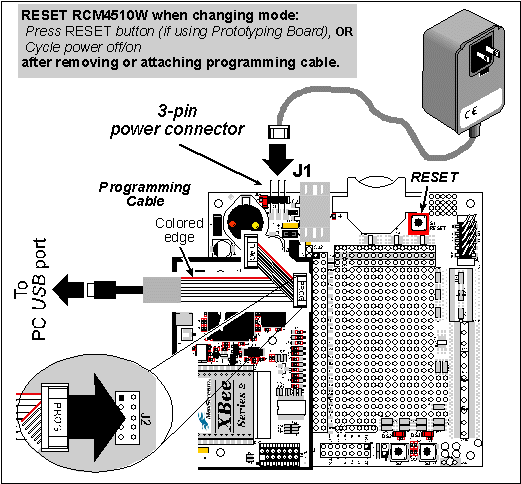
4.3.2 Standalone Operation of the RCM4510W
Once the RCM4510W has been programmed successfully, remove the programming cable from the programming connector and reset the RCM4510W. The RCM4510W may be reset by cycling, the power off/on or by pressing the RESET button on the Prototyping Board. The RCM4510W module may now be removed from the Prototyping Board for end-use installation.
4.4 Auxiliary I/O
4.4.1 Digital I/O
The RCM4510W modules' XBee RF module has up to five general-purpose I/O on header J4 — GPIO0, GPIO8, GPIO13, GPIO15, and GPIO16. Table 4 provides the names used in Dynamic C for these pins and their default configurations.
Table 4. XBee RF Module GPIO Pin Setup J4 Pin Schematic Name Dynamic C Name Default Configuration
All the pins have the following software-configurable features.
- Selectable as input or output.
- Output is either sinking or sourcing, and may be set up for a default high or low.
- Can be pulled up internally.
The four digital I/O, DIO0–DIO3, are similar to the general-purpose I/O, but may instead by configured in software as analog inputs.
NOTE The XBee firmware associated with Dynamic C v. 10.46 does not support I/O reads for RCM4510W RabbitCore modules set up as API coordinators or as API routers. The input switching threshold between logic 0 and logic 1 is 0.66–2.64 V DC, and the output switching threshold between logic 0 and logic 1 is 0.59–2.71 V DC.
4.4.2 A/D Converter
The RCM4510W modules' XBee RF module has four inputs on header J4 that may be set up in software as analog inputs.
The four analog input pins, ADC0–ADC3, each have an input impedance of 6–7 MW, depending on whether they are used as single-ended or differential inputs. The input signal can range from -1.2 V to +1.2 V (differential mode) or from 0 V to +1.2 V (single-ended mode).
Use a resistor divider such as the one shown in Figure 10 to measure voltages above 1.2 V on the analog inputs.
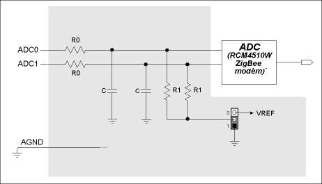
The R1 resistors are typically 20 kW to 100 kW, with a lower resistance leading to more accuracy, but at the expense of a higher current draw. The R0 resistors would then be 180 kW to 900 kW for a 10:1 attenuator. The capacitor filters noise pulses on the A/D converter input.
The A/D converter can only accept positive voltages. With the R1 resistors connected to ground, your analog circuit is well-suited to perform positive A/D conversions. When the R1 resistors are tied to ground for differential measurements, both differential inputs must be referenced to analog ground, and both inputs must be positive with respect to analog ground.
If a device such as a battery is connected across two channels for a differential measurement, and it is not referenced to analog ground, then the current from the device will flow through both sets of attenuator resistors without flowing back to analog ground as shown in Figure 11. This will generate a negative voltage at one of the inputs, ADC1, which will almost certainly lead to inaccurate A/D conversions. To make such differential measurements, connect the R1 resistors to the A/D converter's internal reference voltage, which is 1.2 V. This internal reference voltage can be configured in software to be available on pin 6 of header J4 as VREF, and allows you to convert analog input voltages that are negative with respect to analog ground.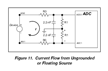
4.4.3 Other Pin Features
There are two other features brought out on the auxiliary I/O header J4.
- There is a +3.3 V power supply point on pin 8, which can deliver up to 25 mA at 3.3 V DC. This power supply point is essentially a filtered and isolated version of the regulated +3.3 V DC power that is supplied to the RCM4510W RabbitCore module through pin 1 of header J1 from the motherboard.
- The SYS_PWR_ON signal on pin 9 is used by the XBee RF module to place the remaining circuitry on the RCM4510W RabbitCore module into a powered-down "sleep" mode or to bring it back up to normal operation.
4.5 Other Hardware
4.5.1 Clock Doubler
The clock doubler on the RCM4510W is disabled by default.
4.5.2 Spectrum Spreader
The Rabbit 4000 features a spectrum spreader, which helps to mitigate EMI problems. The spectrum spreader is on by default, but it may also be turned off or set to a stronger setting. The means for doing so is through a simple configuration macro as shown below.
NOTE Refer to the Rabbit 4000 Microprocessor User's Manual for more information on the spectrum-spreading setting and the maximum clock speed. 4.6 Memory
4.6.1 SRAM
All RCM4510W modules have 512K of battery-backed data SRAM installed at U4.
4.6.2 Flash EPROM
All RCM4510W modules also have 512K of flash EPROM installed at U3.
NOTE Rabbit recommends that any customer applications should not be constrained by the sector size of the flash EPROM since it may be necessary to change the sector size in the future. Writing to arbitrary flash memory addresses at run time is discouraged. Instead, define a "user block" area to store persistent data. The functions
writeUserBlockandreadUserBlockare provided for this. Refer to the Rabbit 4000 Microprocessor Designer's Handbook for additional information.
| Rabbit—A Digi International Brand www.rabbit.com |
