
User's Manual
|
| RabbitCore RCM4500W User's Manual |
Appendix A. RCM4510W Specifications
Appendix A provides the specifications for the RCM4510W, and describes the conformal coating.
A.1 Electrical and Mechanical Characteristics
Figure A-1 shows the mechanical dimensions for the RCM4510W.
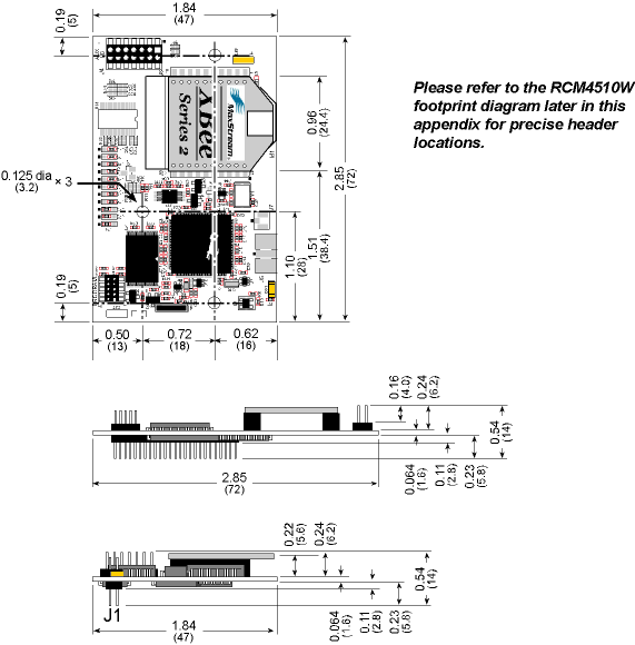
NOTE All measurements are in inches followed by millimeters enclosed in parentheses. All dimensions have a manufacturing tolerance of ±0.01" (0.25 mm). It is recommended that you allow for an "exclusion zone" of 0.04" (1 mm) around the RCM4510W in all directions when the RCM4510W is incorporated into an assembly that includes other printed circuit boards. An "exclusion zone" of 0.08" (2 mm) is recommended below the RCM4510W when the RCM4510W is plugged into another assembly. Figure A-2 shows this "exclusion zone."
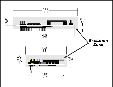
Table A-1 lists the electrical, mechanical, and environmental specifications for the RCM4510W.
Table A-1. RCM4510W Specifications Parameter RCM4510W Microprocessor
Flash Memory
Data SRAM
Backup Battery
General Purpose I/O
up to 49 parallel digital I/0 lines:
· up to 40 Rabbit 4000 pins configurable with four layers of alternate functions
· up to 9 XBee RF module pins, four of which may be configured as analog inputs1
Additional Inputs
Additional Outputs
Analog Inputs*
External I/O Bus
Serial Ports
6 high-speed, CMOS-compatible ports:
Serial Rate
Slave Interface
Slave port allows the RCM4510W to be used as an intelligent peripheral device slaved to a master processor
Real Time Clock
Timers
Watchdog/Supervisor
Pulse-Width Modulators
4 channels synchronized PWM with 10-bit counter
4 channels variable-phase or synchronized PWM with 16-bit counter
Input Capture
Quadrature Decoder
Power with ZigBee® Modem
(pins unloaded)
Operating Temperature
Humidity
Connectors
Board Size with XBee RF module Installed
XBee RF Module RF Module
Compliance
1 These I/O pins from the XBee RF module are available on auxiliary I/O header J4.
A.1.1 XBee RF Module
Table A-2 shows the XBee RF module specifications.
The XBee RF module that consists of discrete components on the preview versions of the RCM4510W module has the same specifications.
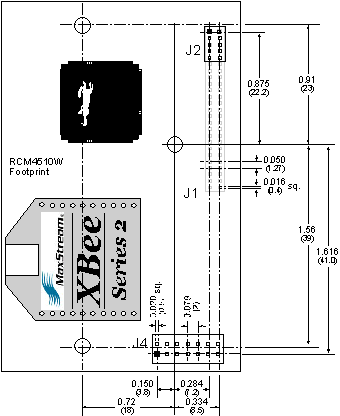
A.1.2 Headers
The RCM4510W uses a header at J1 for physical connection to other boards. J1 is a 2 × 25 SMT header with a 1.27 mm pin spacing. J2, the programming port, is a 2 × 5 header with a 1.27 mm pin spacing. Header J4 supplies auxiliary I/O supported by the XBee RF module, and is a 2 × 7 SMT header with a 2 mm pin spacing
Figure A-3 shows the layout of another board for the RCM4510W to be plugged into. These reference design values are relative to one of the mounting holes.
A.2 Rabbit 4000 DC Characteristics
Table A-3. Rabbit 4000 Absolute Maximum Ratings Symbol Parameter Maximum Rating Operating Temperature
Storage Temperature
Maximum Input Voltage
Maximum Operating Voltage
Stresses beyond those listed in Table A-3 may cause permanent damage. The ratings are stress ratings only, and functional operation of the Rabbit 4000 chip at these or any other conditions beyond those indicated in this section is not implied. Exposure to the absolute maximum rating conditions for extended periods may affect the reliability of the Rabbit 4000 chip.
Table A-4 outlines the DC characteristics for the Rabbit 4000 at 3.3 V over the recommended operating temperature range from TA = –40°C to +85°C, VDDIO = 3.0 V to 3.6 V.
A.3 I/O Buffer Sourcing and Sinking Limit
Unless otherwise specified, the Rabbit I/O buffers are capable of sourcing and sinking 8 mA of current per pin at full AC switching speed. Full AC switching assumes a 29.4 MHz CPU clock with the clock doubler enabled and capacitive loading on address and data lines of less than 70 pF per pin. The absolute maximum operating voltage on all I/O is 3.6 V.
A.4 Bus Loading
You must pay careful attention to bus loading when designing an interface to the RCM4510W. This section provides bus loading information for external devices.
Table A-5 lists the capacitance for the various RCM4510W I/O ports.
Table A-5. Capacitance of Rabbit 4000 I/O Ports I/O Ports Input Capacitance
(pF)Output Capacitance
(pF)Parallel Ports A to E
Table A-6 lists the external capacitive bus loading for the various RCM4510W output ports. Be sure to add the loads for the devices you are using in your custom system and verify that they do not exceed the values in Table A-6.
Table A-6. External Capacitive Bus Loading -40°C to +85°C Output Port Clock Speed (MHz) Maximum External Capacitive Loading (pF) All I/O lines with clock doubler enabled
Figure A-4 shows a typical timing diagram for the Rabbit 4000 microprocessor external I/O read and write cycles.
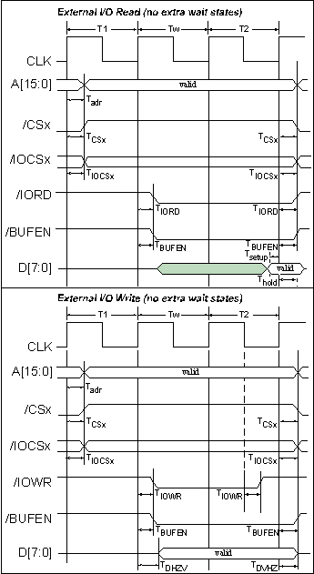
NOTE /IOCSx can be programmed to be active low (default) or active high. Table A-7 lists the delays in gross memory access time for several values of VDDIO.
The measurements are taken at the 50% points under the following conditions.
The clock to address output delays are similar, and apply to the following delays.
- Tadr, the clock to address delay
- TCSx, the clock to memory chip select delay
- TIOCSx, the clock to I/O chip select delay
- TIORD, the clock to I/O read strobe delay
- TIOWR, the clock to I/O write strobe delay
- TBUFEN, the clock to I/O buffer enable delay
The data setup time delays are similar for both Tsetup and Thold.
When the spectrum spreader is enabled with the clock doubler, every other clock cycle is shortened (sometimes lengthened) by a maximum amount given in the table above. The shortening takes place by shortening the high part of the clock. If the doubler is not enabled, then every clock is shortened during the low part of the clock period. The maximum shortening for a pair of clocks combined is shown in the table.
Technical Note TN227, Interfacing External I/O with Rabbit Microprocessor Designs, contains suggestions for interfacing I/O devices to the Rabbit 4000 microprocessors.
A.5 Conformal Coating
The areas around the 32 kHz real-time clock crystal oscillator have had the Dow Corning silicone-based 1-2620 conformal coating applied. The conformally coated area is shown in Figure A-5. The conformal coating protects these high-impedance circuits from the effects of moisture and contaminants over time.
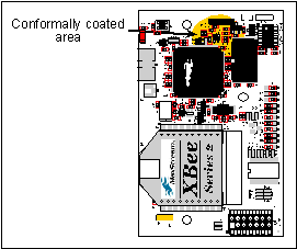
Any components in the conformally coated area may be replaced using standard soldering procedures for surface-mounted components. A new conformal coating should then be applied to offer continuing protection against the effects of moisture and contaminants.
NOTE For more information on conformal coatings, refer to Rabbit's Technical Note TN303, Conformal Coatings, which is included with the online documentation. A.6 Jumper Configurations
Figure A-6 shows the header locations used to configure the various RCM4510W options via jumpers.
Table A-8 lists the configuration options.
NOTE The jumper connections are made using 0 W surface-mounted resistors.
| Rabbit—A Digi International Brand www.rabbit.com |