
User's Manual
|
| RabbitCore RCM4500W User's Manual |
Appendix B. Prototyping Board
Appendix B describes the features and accessories of the Prototyping Board, and explains the use of the Prototyping Board to demonstrate the RCM4510W and to build prototypes of your own circuits. The Prototyping Board has power-supply connections and also provides some basic I/O peripherals (RS-232, LEDs, and switches), as well as a prototyping area for more advanced hardware development.
B.1 Introduction
The Prototyping Board included in the Development Kit makes it easy to connect an RCM4510W module to a power supply and a PC workstation for development. It also provides some basic I/O peripherals (RS-232, LEDs, and switches), as well as a prototyping area for more advanced hardware development.
For the most basic level of evaluation and development, the Prototyping Board can be used without modification.
As you progress to more sophisticated experimentation and hardware development, modifications and additions can be made to the board without modifying the RCM4510W module.
The Prototyping Board is shown below in Figure B-1, with its main features identified.
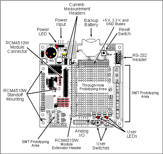
B.1.1 Prototyping Board Features
- Power Connection—A a 3-pin header is provided for connection to the power supply. Note that the 3-pin header is symmetrical, with both outer pins connected to ground and the center pin connected to the raw V+ input. The cable of the AC adapter provided with the North American version of the Development Kit is terminated with a header plug that connects to the 3-pin header in either orientation. The header plug leading to bare leads provided for overseas customers can be connected to the 3-pin header in either orientation.
Users providing their own power supply should ensure that it delivers 8–24 V DC at 8 W. The voltage regulators will get warm while in use.
- Regulated Power Supply—The raw DC voltage provided at the 3-pin header is routed to a 5 V switching voltage regulator, then to a separate 3.3 V linear regulator. The regulators provide stable power to the RCM4510W module and the Prototyping Board.
- Power LED—The power LED lights whenever power is connected to the Prototyping Board.
- Reset Switch—A momentary-contact, normally open switch is connected directly to the RCM4510W's /RESET_IN pin. Pressing the switch forces a hardware reset of the system.
- I/O Switches and LEDs—Two momentary-contact, normally open switches are connected to the PB4 and PB5 pins of the RCM4510W module and may be read as inputs by sample applications.
Two LEDs are connected to the PB2 and PB3 pins of the RCM4510W module, and may be driven as output indicators by sample applications.
- Prototyping Area—A generous prototyping area has been provided for the installation of through-hole components. +3.3 V, +5 V, and Ground buses run around the edge of this area. Several areas for surface-mount devices are also available. (Note that there are SMT device pads on both top and bottom of the Prototyping Board.) Each SMT pad is connected to a hole designed to accept a 30 AWG solid wire.
- Module Extension Header—The complete pin set of the RCM4510W module is duplicated at header J2. Developers can solder wires directly into the appropriate holes, or, for more flexible development, a 2 × 25 header strip with a 0.1" pitch can be soldered into place. See Figure B-4 for the header pinouts.
NOTE The same Prototyping Board can be used for several series of RabbitCore modules, and so the signals at J2 depend on the signals available on the specific RabbitCore module.
- Analog Inputs Header—The analog signals from the RabbitCore module are presented at header J3 on the Prototyping Board. These analog signals are connected via attenuator/filter circuits on the Prototyping Board to the corresponding analog inputs on the RCM4510W module.
- RS-232—Two 3-wire or one 5-wire RS-232 serial ports are available on the Prototyping Board at header J4. A 10-pin 0.1" pitch header strip installed at J4 allows you to connect a ribbon cable that leads to a standard DE-9 serial connector.
- Current Measurement Option—You may cut the trace below header JP1 on the bottom side of the Prototyping Board and install a 1 × 2 header strip from the Development Kit to allow you to use an ammeter across the pins to measure the current drawn from the +5 V supply. Similarly, you may cut the trace below header JP2 on the bottom side of the Prototyping Board and install a 1 × 2 header strip from the Development Kit to allow you to use an ammeter across the pins to measure the current drawn from the +3.3 V supply.
- Backup Battery—A 2032 lithium-ion battery rated at 3.0 V, 220 mA·h, provides battery backup for the RCM4510W SRAM and real-time clock.
B.2 Mechanical Dimensions and Layout
Figure B-2 shows the mechanical dimensions and layout for the Prototyping Board.
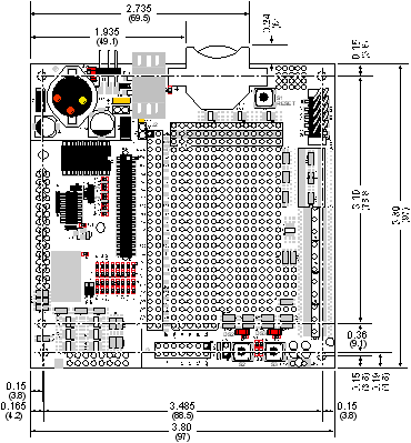
NOTE All measurements are in inches followed by millimeters enclosed in parentheses. All dimensions have a manufacturing tolerance of ±0.01" (0.25 mm). Table B-1 lists the electrical, mechanical, and environmental specifications for the Prototyping Board.
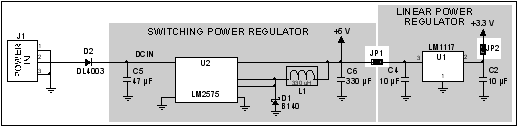
B.3 Power Supply
The RCM4510W requires a regulated 3.0 V – 3.6 V DC power source to operate. Depending on the amount of current required by the application, different regulators can be used to supply this voltage.
The Prototyping Board has an onboard +5 V switching power regulator from which a +3.3 V linear regulator draws its supply. Thus both +5 V and +3.3 V are available on the Prototyping Board.
The Prototyping Board itself is protected against reverse polarity by a Shottky diode at D2 as shown in Figure B-3.
B.4 Using the Prototyping Board
The Prototyping Board is actually both a demonstration board and a prototyping board. As a demonstration board, it can be used to demonstrate the functionality of the RCM4510W right out of the box without any modifications to either board.
The Prototyping Board comes with the basic components necessary to demonstrate the operation of the RCM4510W. Two LEDs (DS2 and DS3) are connected to PB2 and PB3, and two switches (S2 and S3) are connected to PB4 and PB5 to demonstrate the interface to the Rabbit 4000 microprocessor. Reset switch S1 is the hardware reset for the RCM4510W.
The Prototyping Board provides the user with RCM4510W connection points brought out conveniently to labeled points at header J2 on the Prototyping Board. Although header J2 is unstuffed, a 2 × 25 header is included in the bag of parts. RS-232 signals (Serial Ports C and D) are available on header J4. A header strip at J4 allows you to connect a ribbon cable, and a ribbon cable to DB9 connector is included with the Development Kit. The pinouts for these locations are shown in Figure B-4.
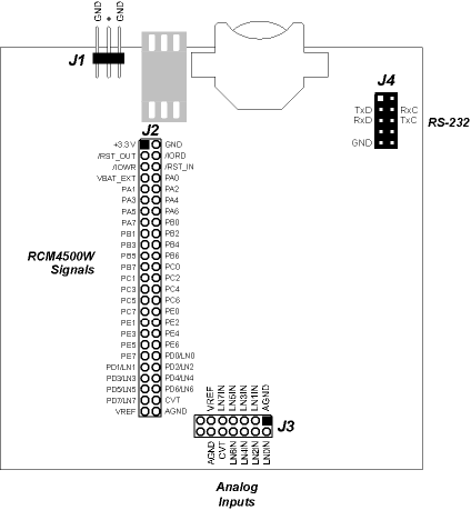
Although analog signals are shown for labeled points at header location J3 on the Prototyping Board, the analog signals on the RCM4510W are associated with the XBee RF module. These analog signals are not brought out to the Prototyping Board.
All signals from the RCM4510W module are available on header J2 of the Prototyping Board. The remaining ports on the Rabbit 4000 microprocessor are used for RS-232 serial communication. Table B-2 lists the signals on header J2 and, where applicable, explains how they are configured by the
brdInit()function call for use on the Prototyping Board.
There is a 1.3" × 2" through-hole prototyping space available on the Prototyping Board. The holes in the prototyping area are spaced at 0.1" (2.5 mm). +3.3 V, +5 V, and GND traces run along the top edge of the prototyping area for easy access. Small to medium circuits can be prototyped using point-to-point wiring with 20 to 30 AWG wire between the prototyping area, the +3.3 V, +5 V, and GND traces, and the surrounding area where surface-mount components may be installed. Small holes are provided around the surface-mounted components that may be installed around the prototyping area.
B.4.1 Adding Other Components
There are pads for 28-pin TSSOP devices, 16-pin SOIC devices, and 6-pin SOT devices that can be used for surface-mount prototyping with these devices. There are also pads that can be used for SMT resistors and capacitors in an 0805 SMT package. Each component has every one of its pin pads connected to a hole in which a 30 AWG wire can be soldered (standard wire wrap wire can be soldered in for point-to-point wiring on the Prototyping Board). Because the traces are very thin, carefully determine which set of holes is connected to which surface-mount pad.
B.4.2 Measuring Current Draw
The Prototyping Board has a current-measurement feature available at header locations JP1 and JP2 for the +5 V and +3.3 V supplies respectively. To measure current, you will have to cut the trace on the bottom side of the Prototyping Board corresponding to the power supply or power supplies whose current draw you will be measuring. Header locations JP1 and JP2 are shown in Figure B-5. Then install a 1 × 2 header strip from the Development Kit on the top side of the Prototyping Board at the header location(s) whose trace(s) you cut. The header strip(s) will allow you to use an ammeter across their pins to measure the current drawn from that supply. Once you are done measuring the current, place a jumper across the header pins to resume normal operation.
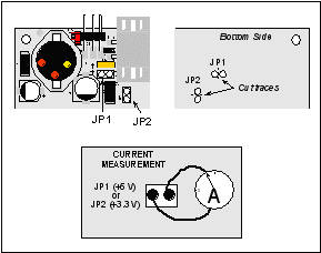
NOTE Once you have cut the trace below header location JP1 or JP2, you must either be using the ammeter or have a jumper in place in order for power to be delivered to the Prototyping Board. B.4.3 Analog Features
The Prototyping Board has typical support circuitry installed to complement the ADS7870 A/D converter chip, which is available on other RabbitCore modules based on the Rabbit 4000 microprocessor, but is not installed on the RCM4510W model. The analog inputs from the auxiliary I/O on the RCM4510W's header J4 cannot be used with the Prototyping Board without modifying the Prototyping Board.
B.4.4 Serial Communication
The Prototyping Board allows you to access the serial ports from the RCM4510W module. Table B-3 summarizes the configuration options.
Table B-3. Prototyping Board Serial Port Configurations Serial Port Header Default Use Alternate Use
Serial Ports E and F may be used as serial ports, or the corresponding pins at header location J2 may be used as parallel ports.
B.4.4.1 RS-232
RS-232 serial communication on header J4 on both Prototyping Boards is supported by an RS-232 transceiver installed at U3. This transceiver provides the voltage output, slew rate, and input voltage immunity required to meet the RS-232 serial communication protocol. Basically, the chip translates the Rabbit 4000's signals to RS-232 signal levels. Note that the polarity is reversed in an RS-232 circuit so that a +3.3 V output becomes approximately -10 V and 0 V is output as +10 V. The RS-232 transceiver also provides the proper line loading for reliable communication.
RS-232 can be used effectively at the RCM4510W module's maximum baud rate for distances of up to 15 m.
RS-232 flow control on an RS-232 port is initiated in software using the
serXflowcontrolOnfunction call fromRS232.LIB, whereXis the serial port (C or D). The locations of the flow control lines are specified using a set of five macros.
SERX_RTS_PORT—Data register for the parallel port that the RTS line is on (e.g., PCDR).
SERA_RTS_SHADOW—Shadow register for the RTS line's parallel port (e.g., PCDRShadow).
SERA_RTS_BIT—The bit number for the RTS line.
SERA_CTS_PORT—Data register for the parallel port that the CTS line is on (e.g., PCDRShadow).
SERA_CTS_BIT—The bit number for the CTS line.Standard 3-wire RS-232 communication using Serial Ports C and D is illustrated in the following sample code.
#define CINBUFSIZE  15   // set size of circular buffers in bytes
#define COUTBUFSIZE 15
#define DINBUFSIZE  15
#define DOUTBUFSIZE 15
#define MYBAUD 115200   // set baud rate
#endif
main(){
    serCopen(_MYBAUD);   // open Serial Ports C and D
    serDopen(_MYBAUD);
    serCwrFlush();       // flush their input and transmit buffers
    serCrdFlush();
    serDwrFlush();
    serDrdFlush();
    serCclose(_MYBAUD);  // close Serial Ports C and D
    serDclose(_MYBAUD);
}
B.5 Prototyping Board Jumper Configurations
Figure B-6 shows the header locations used to configure the various Prototyping Board options via jumpers.
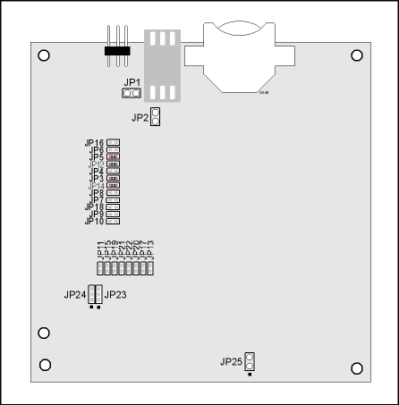
Table B-4 lists the configuration options using either jumpers or 0 W surface-mount resistors.
| Rabbit—A Digi International Brand www.rabbit.com |